Showing posts with label 2. Show all posts
Showing posts with label 2. Show all posts
Saturday, September 6, 2014
TDA1009 Audio Amplifier 2 x 6 W
Description:
Vcc MIN (V)..........9 V
Vcc NOM (V)........14 V
Vcc MAX (V)........24 V
Pout (W)............2 x 6 W
R (Ohm).............4 Ohm
Tip case..............16-DIP+C
Circuit Diagram:
Vcc NOM (V)........14 V
Vcc MAX (V)........24 V
Pout (W)............2 x 6 W
R (Ohm).............4 Ohm
Tip case..............16-DIP+C
Circuit Diagram:
 |
| TDA1009 Circuit Diagram |

Sunday, August 31, 2014
Simple Cell Phone Jammer Wiring diagram Schematic 2
A beautiful diy gsm jammer or mobile cell phone jammer schematic diagram for use only in GSM1900 with frequency from 1930 MHz to 1990 MHz. The GSM1900 mobile phone network is used by USA, Canada and most of the countries in South America.
This cell phone jammier is not applicable for use in Europe, Middle East, nor Asia. The GSM jammier schema could block mobile phone signals which works on GSM1900 band, also called DCS. For more cell phone jammers check the related posts.
Mobile cellphone jammer schema diagram

Tuesday, August 26, 2014
2 Transistor Electronic Siren Wiring diagram Schematic
This is the electronic siren schematic diagram which used 2 transistor BC547 and BC557. The siren is powered by 9V battery or power supply adapter and use 8 ohm speaker to produce the sound. The siren is controlled by the touch plate switch. If you touch the plate, then this electronic siren will be activated.
2 Transistor Electronic Siren Circuit Diagram
Sunday, August 24, 2014
2 X 40 Watt STK amplifier
Components of the above is one component of ic which is applied as a reinforcement. Power amplifier used in an audio signal in order to become more powerful and can be heard via a tool that is the speaker. But in each set must have a voice amplifier, voltage, power quality is different.
For the IC has the output power above 2 X 40 Watt with 8 Ohm output impedance. Supply voltage ranging from 18 Volt to 32 Volt.
For the IC has the output power above 2 X 40 Watt with 8 Ohm output impedance. Supply voltage ranging from 18 Volt to 32 Volt.
Part List
Resistor
R1_____1K
R2_____1K
R3_____22K
R4_____22KR5_____1K2
R6_____100K
R7_____560R
R8_____1K
R9_____1K
R10____470R
R11____4R7
R12____3K3
R13____3K3
R14____4R7
R15____470R
R16____100R
R17____100K
R18____1K2
Capacitor
C1_____470pF
C2_____470pFC3_____4u7F
C4_____4u7F
C5_____82pF
C6_____82pF
C7_____47uF
C8_____100uF
C9_____10nF
C10____39pF
C11____100nF
C12____47uF
C13____47uFC14____100nF
C15____39pFC16____10nF
C17____100uF
C18____47uF
Intregated Circuit
U1_____STK4773 , STK4793 , STK4803 , STK4813 , 4833 , 4843 , 4853 , 4863 , 4873 , 4893 , 4913.
On every IC that I mentioned has a different power output.
Saturday, August 23, 2014
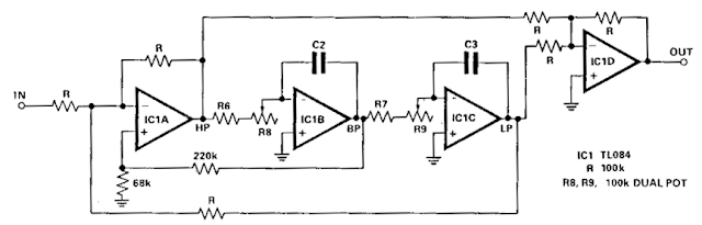
Build an Audio notch filter 2
Build an Audio notch filter 2 Circuit Diagram. With the schema shown here the response at one octave off tune is within 10% of the far out response: notch sharpness may be increased or reduced by reducing or increasing.respectively the 68 ohm resistor. Linearity tracking of R8 and R9 has no effect on notch depth. The signals at HP and LP are always in antiphase, notch will always be very deep at the tuned frequency, despite tolerance variations in R6-9 and C2, C3.
Friday, August 22, 2014
Power Supply 1 2 12V 1A with low voltage LED Indicator

This power supply can provide output voltage 1.2V - 12 with maximal output current is 1A, low voltage LED indicator added in this schematic diagram. The indicator part includes three diodes and one LED. For example you are charging a battery, you can observe the charge status at that moment. Another advantage of this schema, when the drawn current exceeds 1A (practically 0.85A), the current protector in LM317 intervenes and LED indicator warns you about the very low output voltage.
Subscribe to:
Posts (Atom)
