Showing posts with label diagram. Show all posts

Friday, December 12, 2014

Electronic liquid detector circuit diagram


This electronic liquid detector circuit diagram is based on the ULN2429A monolithic bipolar integrated circuit designed for detecting the absence or presence of many different types of liquids. The ULN2429 electronic liquid detector circuit can be used in automotive , home or industrial applications . 
Read More..

Thursday, November 13, 2014

12V fixed voltage power supply circuit diagram

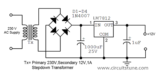
Here this circuit diagram is for +12V regulated (fixed voltage) DC power supply. These power supply circuit diagram is ideal for an average current requirement of  1Amp. This  circuit is based on IC LM7812. It is a 3-terminal (+ve) voltage regulator IC. It has short circuit  protection , thermal overload protection.  LM7812 IC is from LM78XX series. The LM78XX series IC is  positive voltage regulator IC for different voltage requirements, for example LM7805 IC is made for 5 volt fixed output voltage . There is LM79XX IC series for negative voltage .

Circuit diagram of 12V fixed voltage power supply


A transformer(Tx=Primary 230 Volt, Secondary 12 Volt , 1Amp step down transformer) is used to covert 230V to 12V from mains. Here used a bridge rectifier made by four  1N4007 or 1N4003 diode to convert AC to DC . The filtering capacitor 1000uF,25V is used to reduce the ripple and  get a smooth DC voltage. This circuit is very easy to build. For good performance input  voltage should be greater than 12Volt in pin-1 of IC LM7812. Use a heat sink to IC LM7812 for safeguarding it  from overheating.


12
Fig: 12V power supply circuit diagram
Read More..

Thursday, November 6, 2014

Off Line Telephone Tester Circuit Diagram

Here is a circuit of an off-line telephone tester which does not require any telephone line for testing a telephone instrument. The circuit is so simple that it can be easily assembled even by a novice having very little knowledge of electronics. A telephone line may be considered to be a source of some 50 volts DC with a source impedance of about 1 kilo-ohm. During ringing, in place of DC, an AC voltage of 70 to 80 volts (at 17 to 25 Hz) is present across the telephone line. When the subscriber lifts the handset, the same is sensed by the telephone exchange and the ringing AC voltage is disconnected and DC is reconnected to the Off Line Telephone Tester Circuit Diagram line. Lifting of the handset from the telephone cradle results in shunting of the line’s two wires by low impedance of the telephone instrument. As a result, 50V DC level drops to about 12 volts across the telephone instrument.

During conversation, the audio gets superimposed on this DC voltage. Since any DC supply can be used for testing a telephone instrument, the same is derived here from AC mains using step-down transformer X1. Middle point of the transformer’s secondary has been used as common for the two full-wave rectifiers—one comprising diodes D1 and D2 together with smoothing capacitor C1 and the other formed by diodes D3 and D4 along with filter capacitor C2. The former supplies about 12 volts for the telephone instrument through primary of transformer X2 which thus simulates a source impedance, and a choke which blocks AC audio signals present in the secondary of transformer X2. The AF signal available in secondary of X2 is sufficiently strong to directly drive a 32-ohm headset which is connected to the circuit through headphone socket SK1 via rotary switch S2. During ringing, a pulsating DC voltage from transformer X1 via rectifier diode D5, push-to-on switch S3, and contact ‘B’ of rotary switch S2 is applied across secondary of transformer X2.

The boosted voltage available across primary of transformer X2 is sufficient to drive the ringer in the telephone instrument. Please avoid pressing of switch S3 for more than a few seconds at a time to prevent damage to the circuit due to high voltage across primary of transformer X2. The circuit also incorporates a music IC (UM66) whose output is connected to secondary of transformer X2 via switch S2 after suitably boosting its output with the help of darlington transistor pair T1 and T2. This output can be used to test the audio section of any telephone instrument. After having assembled the circuit satisfactorily, the following procedure may be followed for testing a telephone instrument: 1. Connect the telephone to the terminals marked ‘To Telephone Under Test’and switch on mains (switch S1). 2. To test the ringer portion, flip switch S2 to position ‘B’ and press S3 for a moment. You should hear the ring in case the ringer circuit of the telephone under test is working. Please ensure that handset is on cradle during this test. 3. For testing the audio section, flip switch S1 to position ‘C’ and connect a headphone to socket SK1.

Pick the telephone handset and speak into its microphone. If audio section is working satisfactorily, you should be able to hear your speach via the headphone. If you dial a number, you should be able to hear the pulse clicks or pulse tone in the headphone, depending on whether the telephone under test is functioning in pulse or tone mode. If the telephone under test has a built-in musical hold facility, on pressing the ‘hold’ button you should be able to hear the music. Now flip switch S2 to position ‘A’. You should be able to hear music generated by IC1 through earpiece of the handset of the telephone under test, indicating propor functioning of the AF amplifier section. The circuit can be assembled on a small piece of veroboard. Try to mount the two transformers on opposite sides of the board, displaced by 90 degrees. Always keep handy multi-type modular plugs for testing various types of telephones. Mount all switches, sockets and LEDs on the front of testing panel
Read More..

Thursday, October 30, 2014

Speech Filter Circuit Diagram

In communications receivers and microphone amplifiers for transmitting equipment, there is frequently a need for a narrow, low-frequency band-pass filter that lets only the voice band through. This band is usually defined to be the portion of the audio frequency spectrum between approximately 300 Hz and 3300 Hz. In order to implement such a filter, we have calculated the values for two fifth-order Butterworth filters having these corner frequencies and connected them in series. The result is a band-pass filter for the desired pass-band with a skirt steepness of 100 dB/decade.  The first opamp (IC1) acts as a buffer.

Speech Filter Image :

 
image


The circuit can be powered by a unipolar supply voltage between 5 V and 18 V, which is a broad enough range that it should always be possible to find a suitable voltage when building the filter into existing equipment. The current consumption of the filter is only a few milliampères, which should rarely pose a problem. There is fairly wide selection of suitable candidates for the opamps, since the circuit is not critical in this regard. In addition to the indicated OP27A, you could consider using a TL081N or even an old-fashioned 741.

Speech Filter Circuit diagram : 
Speech-Filter-Circut-Diagram
Speech Filter Circuit Diagram 


Due to unavoidable spreads in component values, the pass-band curve of the filter will never be completely perfect in actual practice. However, the deviations will be very small and in any case inaudible. In the pass-band region, the gain is approximately unity. The printed circuit board design shown here allows the speech filter to be built in a very compact form, which can be an important factor if it must be fitted into existing equipment. You can quickly check the fully assembled circuit by momentarily measuring the voltages at the inputs and out-puts of the three opamps. Half of the supply voltage should be present at all of these locations.

PCB Layout :


Parts LIST:
Resistors:
R1.R2 = 22kΩ
R3,R11,R12,R18,R19 = 100kΩ
R4 = 470Ω
R5 = 150Ω
R6 = 10kΩ
R7 = 18kΩ
R8 = 15kΩ
R9 = 33kΩ
R10 = 82kΩ
R13-R17 = 3kΩ3
Capacitors:
C1,C8,C14,C15 = 100nF
C2 = 1µF MKT
C3-C7,C11 = 22nF
C9 = 33nF
C10 = 18nF
C12 = 10nF
C13 = 4nF7
C16,C17 = 10µF 16V
Semiconductors:
IC1,IC2,IC3 = OP27A, TL081CN
Miscellaneous:
Bt1 = 9-V battery


Author: G.Baars
Read More..

Tuesday, October 28, 2014

Cell Phone Detector circuit diagram

The circuit can detect both the incoming and outgoing calls, SMS and video transmission even if the mobile phone is kept in the silent mode. The moment the bug detects RF transmission signal from an activated mobile phone, it starts sounding a beep alarm and the LED blinks. The alarm continues until the signal transmission ceases.
An ordinary RF detector using tuned LC circuits is not suitable for detecting signals in the GHz frequency band used in mobile phones. The transmission frequency of mobile phones ranges from 0.9 to 3 GHz with a wavelength of 3.3 to 10 cm. So a circuit detecting gigahertz signals is required for a mobile bug.

Here the circuit uses a 0.22μF disk capacitor (C3) to capture the RF signals from the mobile phone. The lead length of the capacitor is fixed as 18 mm with a spacing of 8 mm between the leads to get the desired frequency. The disk capacitor along with the leads acts as a small gigahertz loop antenna to collect the RF signals from the mobile phone.
Read More..

Thursday, October 16, 2014

Build a Period To Voltage Converter Circuit Diagram

The input signal drives ICD. Because ICD`s positive input (V+) is slightly offset to + 0.1 V, its steady stateoutput will be around +13 V. This voltage is sent to ICC through D2, setting ICC`s output to +13 V. Therefore, point D is cut off by Dl, and CI is charged by the current source. Assuming the initial voltage on CI is zero, the maximum voltage (^Cinax) is given by: 

When the input goes from low to high, a narrow positive pulse is generated at point A. This pulse becomes -13 V at point B, which cuts off D2. ICC`s V+ voltage becomes zero. The charge on CI will be absorbed by ICC on in a short time. 

The time constant of C2 and R5 determines the discharge period— about 10 /is. ICB is a buffer whose gain is equal to (R& + R9)~Rg = lM5. ICD`s average voltage will be (1362f 1.545) + 2 = 1052/. RIO and C3 smooth the sawtooth waveform to a dc output.


Period-To-Voltage Converter Circuit Diagram

Read More..

Wednesday, October 1, 2014

Stereo Cassette Player Circuit Diagram

As the equipment is mains operated, the battery compartment can be removed. The loudspeaker can also be removed as it is no longer required; the mains transformer may be fitted in its position. lf so desired, you · may add a neon indicator and a mains switch as well. Assembly cost and time As to the cost, you are lucky if you are in Delhi and can shop around Lajpatrai Market. The cost would be around Rs 400 or even less if you know the way the Delhi market works. Outside Delhi, the cost would be around Rs 450 much less than you would pay for a mono cassette recorder. lt is certainly worth every rupee that you spend as it would enable you to use the stereo system that you already own. Assembly time would depend on your familiarity with the electronic circuitry, but it would be a weekend well spent. (Time you need for shopping for the mechanism and parts would be extra.)  Two direct·coupled transistors are used in the preamplifier, with base bias for the first provided from the emitter of the second. This system of biasing results in heavy DC ° feedback that ensures stable operation of the circuit.


With the DC operating conditions stabilised, as mentioned, the AC characteristics of the preamplifier are also stabilised. The AC feedback from the collector of the second A transistor to the emitter of the first mainly provides frequency equalisation high frequency de-emphasis to compensate for the recording characteristics. To keep up a high signal- to-noise ratio in the high frequency range, the highs are boosted during recording. (This is called pre-emphasis.) A reverse treatment is therefore essential in playback to reproduce the original high-frequency signal correctly. An R- C combination, 22k with 5nF capacitor, carries out this function adequately.

Output from the preamplifier is fed to a 741 op-amp set for a gain of about ten. The total gain is thus around 1000 so as to provide a 100mV signal from 100uV input normally expected from a cassette head. Use of discrete preamplifier at the input ensures a good signal-to-noise ratio, and the op-amp at the output with a wide dynamic range ensures that there is no chance of signal being driven into saturation. The signal from the preamp is fed to inverting terminal number 2 of the op-amp through 5.6k resistor. Negative feedback from the output terminal number 6 through 68k is also provided to terminal number 2. The non-inverting terminal number 3 is set to half the supply voltage. That sets the DC voltage at terminal number 6. Thus an optimum swing of the output is possible at terminal number6. Positive supply terminal number 7 is taken to the supply positive, and terminal number 4 returned to ground. The output from the op-amp is taken out through a47k resistor to the standard 3.5 mm socket used in cassette recorders. The socket fits in a window provided in a ‘Sony’ cabinet for mono cassette recorder. `  
Read More..

Saturday, September 20, 2014

Explanation Fuse Box Mercy 2004 C240 Engine Diagram

Fuse Box Mercy 2004 C240 Engine Diagram - Below is Fuse Box Mercy 2004 C240 Engine Diagram.

Fuse Box Mercy 2004 C240 Engine Diagram


Fuse
Fuse

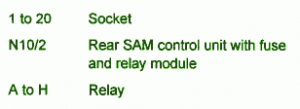
Fuse Panel Layout Diagram Parts: socket, rear SAM control unit, relay, fuse and relay module.
Read More..

Friday, September 19, 2014

Simple and hold circuit using op amp Circuits Wiring diagram

As the name indicates , a sample and hold schema is a schema which samples an input signal and holds onto its last sampled value until the input is sampled again. Sample and hold diagram are commonly used in analogue to digital converts, communication diagram, PWM diagram etc. The schema shown below is of a sample and hold schema based on uA 741 opamp , n-channel E MOSFET BS170 and few passive components.

Description

As the name indicates , a sample and hold schema is a schema which samples an input signal and holds onto its last sampled value until the input is sampled again. Sample and hold diagram are commonly used in analogue to digital converts, communication diagram, PWM diagram etc. The schema shown below is of a sample and hold schema based on uA 741 opamp , n-channel E MOSFET BS170 and few passive components.

In the schema MOSFET BS170 (Q1) works as a switch while opamp uA741 is wired as a voltage follower. The signal to be sampled (Vin) is applied to the drain of MOSFET while the sample and hold control voltage (Vs) is applied to the source of the MOSFET. The source pin of the MOSFET is connected to the non inverting input of the opamp through the resistor R3. C1 which is a polyester capacitor serves as the charge storing device. Resistor R2 serves as the load resistor while preset R1 is used for adjusting the offset voltage.
During the positive half cycle of the Vs, the MOSFET is ON which acts like a closed switch and the capacitor C1 is charged by the Vin and the same voltage (Vin) appears at the output of the opamp. When Vs is zero MOSFET is switched off and the only discharge path for C1 is through the inverting input of the opamp. Since the input impedance of the opamp is too high the voltage Vin is retained and it appears at the output of the opamp.

The time periods of the Vs during which the voltage across the capacitor (Vc) is equal to Vin are called sample periods (Ts) and the time periods of Vs during which the voltage across the capacitor C1 (Vc) is held constant are called hold periods (Th). Taking a close look at the input and output wave forms of the schema will make it easier to understand the working of the schema.

Circuit diagram

 Sample and Hold schema using uA741 opamp

Input and output waveforms.

sample
Input and output waveforms - Sample and hold schema

Notes

  • The schema can be assembled on a vero board.
  • Use +15V/-15V DC dual supply for powering the opamp.
  • Capacitor C1 must have minimum leakage current possible and thats why a polyester capacitor is used here.
  • Mount the IC uA741 on a holder.
  • The type number of the MOSFET Q1 is not very significant here and so substitution is possible if BS170 is not available.
  • BS170 is a 60V, 500mA n-channel enhancement mode MOSFET available in TO-92 package.
  • Preset resistor R1 can be used for offset adjustments.
Read More..

Wednesday, September 17, 2014

How to Build a FM Transmitter Circuit Diagram


How to Build a FM Transmitter Circuit Diagram. Lets start this simple FM Transmitter Circuit Diagram making. FM transmitter circuit schematic with a single transistor. It build with a very few numbers of components include a transistor, few capacitors, resistors and a small microphone. 
 
Read More..

Tuesday, September 16, 2014

Fuse Box Ford 2001 Mustang GT Diagram

Fuse Box Ford 2001 Mustang GT Diagram - Here are new post for Fuse Box Ford 2001 Mustang GT Diagram.

Fuse Box Ford 2001 Mustang GT Diagram


Fuse
Fuse

Fuse Panel Layout Diagram Parts: ABS control module, control relay module, wheel speed sensor, mass air flow, headlamp, fog lamp, park lamp, engine cooling fan, A/C clutch cycling pressure switch, cool on plug.
Read More..

Friday, September 12, 2014

12V Latch Wiring diagram Schematic

This schema controls a solenoid by the operation of a single push-button switch. The schema will supply loads of over 1 A and can be operated up to a maximum speed of once every 0.6 second. When power is first applied to the schema, the solenoid will always start in its off position. Other features of the schema are its automatic turn-off, if the load is shorted, and its virtually zero-power consumption when off.

12V Latch Circuit Diagram

12V

Read More..

Thursday, September 11, 2014

2000 Chevrolet Chevy Blazer Wiring Diagram

2000 Chevrolet Chevy Blazer Wiring Diagram
(More Detail Visit Here)

This is 2000 Chevrolet Chevy Blazer Wiring Diagram: power distribution schematic, fuel pump relay control, fuel pump and sender, splice pack, fuel pump prime connector, ground distribution svhematic, underhood fuse block, vehicle control module, fuel pump relay control..
Read More..

Wednesday, September 10, 2014

Simple Comperator Frequency LED Wiring diagram Schematic

This Simple Comparator Frequency LED Circuit Diagram uses a comparison frequency IC 74HCT00, the device enabling frequency pulses are compared. Frequency F1 (signal frequency channel 1) and F2 (signal frequency channel 2). If the two frequencies are equal, then LED lights.


Comperator Frequency LED Circuit Diagram

Simple


Read More..

Tuesday, September 9, 2014

Precision Full Wave Ac Dc Converter Wiring diagram Schematic

A dc level is produced that corresponds to the ac input rms value (if sine wave), -i set the gain of IC2 to 1.11. This factor is the average-to-rms conversion factor. IC1 and IC2 act as a full-wave rectifier schema, with Dl and D2. 

Precision Full-Wave Ac/Dc Converter Circuit Diagram


Precision
Read More..

Monday, September 8, 2014

Electronic Digital Combination lock Wiring diagram Schematic

Electronic

The schema above above makes use of the CMOS 4017 decade counter IC. Each depression of a switch steps the output through 0– 9. By coupling the output via an AND gate to the next IC, a predefined code has to be input to create the output. Each PBS switch is de bounced by tw1o gates of a CMOS4001 quad 2-input NOR gate. This ensures a clean pulse to the input of each CMOS4017 counter. Only when the correct number of presses at PBS Awill allow PBS B to become active. This is similar for PBS C and PBS D. At IC4, PBS D must be pressed 7 times. Then PBS C is again pressed 7 times, stepping from output 1 to output 8. The AND gate formed around CMOS4081 then goes high, lighting the LED. The Reset switch can be pressed at any time. Power on resetis provided by the 100n capacitor near the reset switch. Below is a picture of one that I made about 15 years ago:  

Super

Unfortunately, this board was part of a much larger project containing multiple power supplies. One day whilst working on another schema , I slipped with a wire and splashed 24volts DConto this board. There was a small spark, and puff of smoke before all this chips were cooked! If anyone does consider building such a schema, then my advice would be to stop and lookin your local electronic parts catalogue. There are now dedicated combination lock IC`s with combinations many time sgreater than this schema. Incidentally the number of combinations offered here is 10 x 10 x 10 x 10 x 9 = 90,000.Check out Dean White`s Electronic Gadgets, on the Electronic Sites Alliance web ring, he also has a combination lock schema.
Read More..

Sunday, September 7, 2014

Simple 1KHz Sine wave Generator Circuits Wiring diagram

This simple schema generates a good 1KHz sine wave adopting the inverted Wain bridge configuration (C1-R3 & C2-R4). It features a variable output, low distortion and low output impedance in order to obtain good overload capability. A small filament bulb ensures a stable long term output amplitude waveform. 

1KHz Sine wave Generator Circuits Diagram


 Notes:
  • The bulb must be a low current type (12V 40-50mA or 6V 50mA) in order to obtain good long term stability and low distortion.
  • Distortion @ 1V RMS output is 0.15% using a 12V 40mA bulb, raising to 0.5% with a 12V 100mA one.
  • Using a bulb differing from specifications may require a change of R6 value to 220 or 150 Ohms to ensure proper diagram oscillation.
  • Set R5 to read 1V RMS on an Audio Millivoltmeter connected to the output with R7 rotated fully clockwise, or to view a sinewave of 2.828V Peak-to-Peak amplitude on the oscilloscope.
  • With C1, C2 = 100nF the frequency generated is 100Hz and with C1, C2 = 1nF frequency is 10KHz but R5 requires adjustment.
  • High gain transistors are preferred for better performance.

Parts:

R1____________5K61/4W Resistor
R2____________1K81/4W Resistor
R3,R4________15K1/4W Resistors
R5__________500R1/2W Trimmer Cermet
R6__________330R1/4W Resistor
R7__________470RLinear Potentiometer
 
C1,C2________10nF63V Polyester Capacitors
C3__________100µF25V Electrolytic Capacitor
C4__________470nF63V Polyester Capacitor
 
Q1,Q2_______BC23825V 100mA NPN Transistors
LP1___________12V40mA Filament Lamp Bulb (See Notes)
 
J1__________Phono chassis Socket
 
SW1__________SPSTSlider Switch
 
B1_____________9VPP3
 
Clip for 9V PP3 Battery

Read More..

Diode Cmos Stabilizer Wiring diagram Schematic

This is the Simple Diode Cmos Stabilizer Circuit Diagram. The simple diode network can stabilize the voltage supplied to CMOS schemary from a battery. D1 and D2 must have a combined forward-voltage drop of about 1.5 V. And D3 is an LED with a forward-voltage drop of about 1.7 V. The table shows the network`s output voltage as the battery`s voltage declines.
 Simple Diode Cmos Stabilizer Circuit Diagram
Simple
 Sourced By: Circuitsstream
Read More..

Saturday, September 6, 2014

Simple Dual Trace Scope Switch Wiring diagram Schematic

Simple Dual Trace Scope Switch Circuit Diagram. The switcher output goes to the single vertical input of the scope, and a sync line from one of the inputs is taken to the scopes external-sync input. Frequency response of the input amplifiers is 300 kHz over the range of the gain controls. With the gain controls wide open so no attenuation of the signal takes place, the frequency response is up to 1 MHz. 

 Simple Dual Trace Scope Switch Circuit Diagram


Simple
Read More..

Simple Electromagnetic Ring Launcher Wiring diagram Schematic

This is a Simple Electromagnetic Ring Launcher Circuit Diagram. The electromagnetic ring launcher is comprised of.four sub diagram: a clock schema (built around U5, a 555 oscillator/timer configured for astable operation), a count-down/display schema (built around U3), a 74190 synchronous up/down counter with BCD outputs that is configured for countdown operation; 

 Simple Electromagnetic Ring Launcher Circuit Diagram


Simple

U4, a ECG8368 BCD-to-7-segment latch/decoder/display driver; and DISP1, a common-cathode seven-segment display), a trigger schema (comprised of U6), an MOC3010 opto isolator/ coupler with Triac-driver output; TR1, an SK3665 200-PIV, 4-A Triac; and a few support components), and a reset schema (comprised of Ul, a 7400 quad 2-input NAND gate U2, a second 555 oscillator/timer configured for monostable operation; and a few support components). This schema is that of a repulsion coil (LI) used to demonstrate the principle of electromagnetic repulsion by propelling a metal ring around the core of LI through the air. A countdown schema is provided to count seconds before launch.
Read More..