Thursday, November 20, 2014

Doubler Digital Frequency

Doubler Digital Frequencycircuit includes a simple and easy to understand. Digital Frequency Doubler circuit application contained in the system electronics such as audio-producing organ, or keyboard. The function of this series Digital Frequency Doubler for multiplying two input frequencies. The process of multiplying 2 on scales in an organ in principle is like this series Digital Frequency Doubler. Example of rising to a ringing tone DO RE then electronically technique in it is by multiplying the two frequency bands such as this series Digital Frequency Doubler.


Doubler
Doubler Digital Frequency
Read More..

Wednesday, November 19, 2014

ADC 0804 Microcontroler Interface Engineering

In ADC 0804 interface techniques with microcontrollers are pin-pin control must be controlled if we want to use the ADC with the microcontroller, there is value addition refferensi voltage to be supplied in 0804 ADC interface with a microcontroller, for example, we use the 0804 ADC (8 bit), if we give refferensi voltage 2.55 volts then we will get the increase of 1 bit to change 10 mVolt. Please note that the 0804 ADC pin on the leg that is form Vref Vref / 2, so to get a 10mV resolution is necessary for setting Vref / 2 equal to 1.275 V

The interface circuit microcontroller with ADC 0804


Mechanical interface microcontroller with ADC 0804
The steps in accessing data from the ADC 0804 by the microcontroller sebgai follows;

Enable ADC with signal 0 at the foot of Chip Select.
Give commands from conversion by providing a low pulse to the foot of the ADC Write narrow
Wait for the ADC issued a signal 0 from his leg INT
Give a moment of time delay for data from the ADC is correct
Give the read command by giving the signal 0 at the foot of ADC Read
Give a moment of time delay Now data from the ADC is ready for use and if the microcontroller.
Read More..

Tuesday, November 18, 2014

Powerful Bat Detector device

PowerfulPowerful Bat Detector device Circuit Diagram

The Powerful Bat Detector is a abundance analysis blazon device. Abundance analysis blazon detectors acquiesce you to apprehend accelerated complete by digitally ascent the abundance bottomward into the animal audition range. For instance, a western pipistrelle bat emits accelerated complete in the ambit of 53 to 91 kHz. If you bisect that abundance by 16, the new abundance ambit is 3.3 to 5.7 kHz, calmly aural our audition range. Because the analysis is done digitally, all amplitude advice is lost. Accelerated sources candy by the detector catechumen to sounds like geiger-counter clicks and chirps.

The basal ambit of the Simple Bat Detector is apparent in the schematic diagram to the right. It is about composed of 3 chip circuits, or ICs. The arresting from an accelerated transducer is fed to IC-1, an LM386 audio amplifier, which is configured to accommodate a arresting accretion of 200. The arresting is accompanying to IC-2, a added LM386, by a .05 uf capacitor. IC-2 is configured to accommodate an added accretion of 20, for a absolute arrangement accretion of 4,000. The achievement of IC-2 is absolute accompanying to the ascribe of IC-3, a 7 date CMOS agenda affiliate circuit. The ascribe date of the affiliate acts as a aught bridge detector, triggering on the abrogating alteration of the arresting from IC-2. The bisect by 16 achievement is affiliated to a potentiometer, which serves as an audio akin control. A aerial impedance bowl earphone is affiliated to the achievement of the akin control. The 10K akin ascendancy is a baby printed ambit pot that is set and forgotten. The detector ambit is powered by a nine volt battery. ( The numbers abutting to the IC nodes accredit to the pin numbers of the ICs. Note the added pins listed at the basal of the schematic that charge to be angry to ground. )

A above advantage of a abundance analysis detector is that it is a advanced bandage accessory ... that agency it will let you apprehend all apparent bat sounds after the charge to tune the detector to any accurate frequency. Heterodyne detectors, which action accelerated complete in the analog domain, alone catechumen a baby ambit of frequencies at any accustomed time - you charge baddest which frequencies to accept to. If you tune up about 60 kHz to accept for a pipistrelle, you may not apprehend the big amber bats aerial nearby. The abundance analysis detector works in the agenda domain, converting the abounding spectrum of complete that the transducer is able to detect. So you get to accept to all of the accelerated sounds about you, after missing annihilation due to adverse affability choices. I feel this no-knobs-needed appropriate of the abundance analysis detector makes it a abundant best for the accidental bat observer, and student.

Read More..

Monday, November 17, 2014

Multiplexer Circuit With Logic Gate

Multiplexer circuit with a logic gate is a multiplexer circuit that utilizes a combination of logic gates.
Where the above example can be seen that the circuit has 2 bit selector and 4 input lines. You can make a circuit with more input channels by increasing the number of bits of the selector. And also you can use a combination of gates based on your own design with reference to the previous multiplexer truth table you should specify. So by making a truth table in advance you can easily create a series of logic gates.


Multiplexer

The working principle of the multiplexer circuit above is:

1. Value of bit 00 from the selector will choose the path of the first input as the output
2. Value of bit 01 of the selector will choose the path of the second input as output
3. Value of bit 10 of the selector selects the third input lines as output
4. Value of bit 11 of the selector will choose the four input channels as output
5. As long as there is no change in the bit selector logic condition of the output logic state also will not be amended.
6. If the line selector is connected with a series of counter-up the output to be obtained will represent the input lines in sequence.
7. So it can be concluded that the usefulness of the implementation of a multiplexer function is to satisfy the principle of a simple data distribution. Thus, with multiplexers is possible to transmit data remotely using only one connection.
Read More..

Saturday, November 15, 2014

100W MOSFET POWER AMPLIFIER

A 100W MOSFET power amplifier circuit based on IRFP240 and IRFP9240 MOSFETs is shown here. The amplifier operates from a +45/-45 V DC dual supply and can deliver 100 watt rms into an 8 ohm speaker and 160 watt rms into a 4 ohm speaker. This Hi-Fi amplifier circuit is suitable for a lot applications like general purpose amplifier, guitar amplifier, keyboard amplifier. The amplifier can be also used as a sub woofer amplifier but a subwoofer filter stage has to be added before the input stage. The amplifier has a low distortion of 0.1%, a damping factor greater than 200, input sensitivity of 1.2V and the bandwidth is from 4Hz to 4 KHz.

Circuit Diagram


About the Circuit

Capacitor C8 is the input DC decoupling capacitor which blocks DC voltage if any from the input source. IF unblocked, this DC voltage will alter the bias setting s of the succeeding stages. Resistor R20 limits the input current to Q1 C7 bypasses any high frequency noise from the input. Transistor Q1 and Q2 forms the input differential pair and the constant current source circuit built around Q9 and Q10 sources 1mA. Preset R1 is used for adjusting the voltage at the output of the amplifier. Resistors R3 and R2 sets the gain of the amplifier. The second differential stage is formed by transistors Q3 and Q6 while transistors Q4 and Q5 forms a current mirror which makes the second differential pair to drain an identical current. This is done in order to improve linearity and gain. Power amplification stage based on Q7 and Q8 which operates in the class AB mode. Preset R8 can be used for adjusting the quiescent current of the amplifier. The network comprising of capacitor C3 and resistor R19 improves high frequency stability and prevents the chance of oscillation. F1 and F2 are safety fuses.

Circuit Setup

Set R1 at midpoint before powering up and then adjust it slowly in order to get a minimum voltage (less than 50mV0 at the output. Next step is setting up the quiescent current and keep the preset R8 in minimum resistance and connect a multimeter across points marked X & Y in the circuit diagram. Now adjust R8 so that the multimeter reads 16.5mV which corresponds to 50mA quiescent current.

Notes

  • Assemble the circuit on a good quality PCB.
  • Use a +45/-45 V DC, 3A dual supply for powering the circuit.
  • Power supply voltage must not exceed +55/-55 V DC.
  • Before connecting the speaker, check the zero signal output voltage of the amplifier and in any case it should not be higher than 50mV. If it is higher than 50mV, check the circuit for any error. Replacing Q1, Q2 with another set could also solve the problem.
  • Fit Q7 and Q8 to a 2°C/W heat sink. Both Q7 and Q8 must be isolated from the heat sink using mica sheets. Heat sink mounting kits for almost all power transistors/ MOSFETs of almost all package styles are readily available in the market.
  • All resistors other than R10, R11 and R19 are 1/4 watt metal film resistors. R10 and R11 are 5W wire wound type while R19 is a 3W wire wound type.


Power Supply for the 100W MOSFET Power Amplifier


Read More..

Thursday, November 13, 2014

12V fixed voltage power supply circuit diagram

Here this circuit diagram is for +12V regulated (fixed voltage) DC power supply. These power supply circuit diagram is ideal for an average current requirement of  1Amp. This  circuit is based on IC LM7812. It is a 3-terminal (+ve) voltage regulator IC. It has short circuit  protection , thermal overload protection.  LM7812 IC is from LM78XX series. The LM78XX series IC is  positive voltage regulator IC for different voltage requirements, for example LM7805 IC is made for 5 volt fixed output voltage . There is LM79XX IC series for negative voltage .

Circuit diagram of 12V fixed voltage power supply


A transformer(Tx=Primary 230 Volt, Secondary 12 Volt , 1Amp step down transformer) is used to covert 230V to 12V from mains. Here used a bridge rectifier made by four  1N4007 or 1N4003 diode to convert AC to DC . The filtering capacitor 1000uF,25V is used to reduce the ripple and  get a smooth DC voltage. This circuit is very easy to build. For good performance input  voltage should be greater than 12Volt in pin-1 of IC LM7812. Use a heat sink to IC LM7812 for safeguarding it  from overheating.


12
Fig: 12V power supply circuit diagram
Read More..

Wednesday, November 12, 2014

ic NE 555 Timer IC Datasheet Applications and Circuit Schematics


NE-555 timer IC was being introduced around May 1971 by the Signetics Corporation, to become known as the NE-555 / SE-555, and was also the very first very mass-produced commercially produced timer IC available at that time. Philips semiconductor was then introduced this 555 timer in mid 1972. Its characteristics for versatility, stability, low cost, simplicity to produce long time delays in a variety of applications, make Electronic Engineers, Circuit Designers from mechanical timers, op amps, and various discrete circuits into the ever increasing ranks of timer users.

Invented by a clever Swiss man, Hans R. Camenzind in 1970, the NE-555 timer IC went on to become a legend in the industry. As we already know, the 555 timer operates in three basic mode: monostable (one shot), astable (oscilatory), and time delay. In the article below each of basic operating mode were described detailly in one sequence with its schematic diagrams.

Another sections you can follow in this datasheet applications are general design consideration of the 555 timer, frequently asked applications question (FAQ), design formulas, and sample of some ingenious applications. The sample of applications were presented such as Missing Pulse Detector, Pulse Width Modulation (PWM), Tone Burst Generator, Long Time Delays, Car Tachometer (click to enlarge the picture above), Auto Burglar Alarm, Cable Tester, Automobile Voltage Regulator, and more. Each sample is given with clear and detail circuit schematic diagrams.

The article is ended with Theory of Operation and The Speed Warning Circuit section. Read on complete information about The NE 555 Timer IC Datasheet Applications and Circuit Schematics with link to download in pdf document provided (source: doctronics.co.uk).

Read More..

Saturday, November 8, 2014

USB Power Booster

The USB serial bus can be configured for connecting several peripheral devices to a single PC. It is more complex than RS232, but faster and simpler for PC expansion.Since a PC can supply only a limited power to the external devices connected through its USB port, when too many devices are connected simultaneously, there is a possibility of power shortage. Therefore an external power source has to be added to power the external devices.
Circuit diagram:
USB Power Booster Circuit Diagram
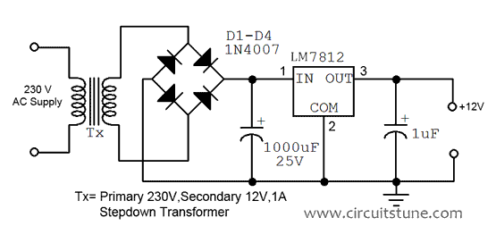
In USB, two different types of connectors are used: type A and type  B. The circuit presented here is an add-on unit, designed to add more power to a USB supply line (type-A). When power signal from the PC (+5V) is received through socket A, LED1 glows, opto-diac IC1 conducts and TRIAC1 is triggered, resulting in availability of mains supply from the primary of transformer X1. Now transformer X1 delivers 12V at its secondary, which is rectified by a bridge rectifier comprising diodes D1 through D4 and filtered by capacitor C2.
 Pin configurations of moc3021, bt136 and 5v regulator 7805 
Regulator 7805 is used to stabilise the rectified DC. Capacitor C3 at the output of the regulator bypasses the ripples present in the rectified DC output. LED1 indicates the status of the USB power booster circuit. Assemble the circuit on a general-purpose PCB and enclose in a suitable cabinet. Bring out the +5V, ground and data points in the type-A socket. Connect the data cables as assigned in the circuit and the USB power booster is ready to function
Read More..

Friday, November 7, 2014

LM723 Variable Power Supply with Over Current Protection

The circuit design was intended to create an adjustable power supply over a range of 1.3V to 12.2V at 1A and be able to provide protection for over-current by utilizing LM723 regulator.


 Terminology
  • LM723 – a positive NPN standard voltage regulator mainly designed for series regulator applications which can be utilized for both foldback and linear current limiting due to its very low standby current drain circuit
  • Voltage Regulator – an electrical or electronic device created for the purpose of maintaining a constant voltage level of a power source within the suitable limits
  • 2N3055 – a complementary Silicon Epitaxial-Base planar NPN transistor mounted in Jedec TO-3 metal case for use as power transistor
Circuit Explanation
The integrated voltage regulator LM723 will supply 150 mA of output currents but any desired load current can be provided by adding external transistors for output currents in excess of 10A. This can be used as a linear or switching regulator since its output voltage can be adjusted from 2 Volts to 37 Volts while the input voltage can be at 40 Volts maximum. The range of variations of input voltage and load current can be kept at constant using this voltage regulator.

In this design, the DIL14 plastic packaged LM723 performs with 9.5V to 40V input DC voltage while having an output voltage that is not more then 6V to 7V below the input will lead to 150 mA current source from  the IC. The difference between the input and the output DC voltage plus the current is proportional to the amount power being dissipated by the transistor T1 as it accepts all the current brought by the load, thus requiring a heatsink with a heat conductive value of 5K/W. T1 is made from 2N3055 which is intended for series and shunt regulators, for output stages and high fidelity amplifiers, and for power switching circuits. The output stage of the integrated circuit will be less loaded when an external pass transistor is used which will conduct at emitter-follower mode. This will in turn cause T1 to conduct at base-emitter mode thereby producing a major resistance in the IC.

Both ceramic capacitors must be positioned closer to the integrated circuit to prevent undesired oscillations, which the LM723 is prone to, since ceramic capacitors have high frequency coefficient of dissipation. Having these capacitors directly soldered would be too much for the IC since the operating temperature of the IC is in the range of -55ᵒC to +125ᵒC

Application
Voltage regulators are used for several advantages in areas where uncontrolled voltage varies more than the accepted voltage of equipment which could be harmful and damaging. In motor vehicles, it matches the charging requirements of the battery and electrical load to the output voltage of the generator by rapidly switching from one to another of three circuit states using a dual pole switch loaded with spring. To keep a recommended range of voltage supplied to a consumer, regulators are used by alternating current distribution feeders or large scale power distributions or substations. This is useful in protecting the equipment using electricity by minimizing the variations in voltage.  The two types of regulators being used are step regulators where the current supply is controlled and the induction regulator where an induction motor adjust the voltage by supplying a secondary which smoothens the feeder line’s current variations.
The LM723 voltage regulators are widely used for wide range of applications such as a temperature controller, a current regulator, or a shunt regulator. Also, DC power supplies in electronic equipment are using voltage regulators.

Source:zen22142.zen.co.uk/Circuits/Power/723psu.htm
Read More..

Thursday, November 6, 2014

Off Line Telephone Tester Circuit Diagram

Here is a circuit of an off-line telephone tester which does not require any telephone line for testing a telephone instrument. The circuit is so simple that it can be easily assembled even by a novice having very little knowledge of electronics. A telephone line may be considered to be a source of some 50 volts DC with a source impedance of about 1 kilo-ohm. During ringing, in place of DC, an AC voltage of 70 to 80 volts (at 17 to 25 Hz) is present across the telephone line. When the subscriber lifts the handset, the same is sensed by the telephone exchange and the ringing AC voltage is disconnected and DC is reconnected to the Off Line Telephone Tester Circuit Diagram line. Lifting of the handset from the telephone cradle results in shunting of the line’s two wires by low impedance of the telephone instrument. As a result, 50V DC level drops to about 12 volts across the telephone instrument.

During conversation, the audio gets superimposed on this DC voltage. Since any DC supply can be used for testing a telephone instrument, the same is derived here from AC mains using step-down transformer X1. Middle point of the transformer’s secondary has been used as common for the two full-wave rectifiers—one comprising diodes D1 and D2 together with smoothing capacitor C1 and the other formed by diodes D3 and D4 along with filter capacitor C2. The former supplies about 12 volts for the telephone instrument through primary of transformer X2 which thus simulates a source impedance, and a choke which blocks AC audio signals present in the secondary of transformer X2. The AF signal available in secondary of X2 is sufficiently strong to directly drive a 32-ohm headset which is connected to the circuit through headphone socket SK1 via rotary switch S2. During ringing, a pulsating DC voltage from transformer X1 via rectifier diode D5, push-to-on switch S3, and contact ‘B’ of rotary switch S2 is applied across secondary of transformer X2.

The boosted voltage available across primary of transformer X2 is sufficient to drive the ringer in the telephone instrument. Please avoid pressing of switch S3 for more than a few seconds at a time to prevent damage to the circuit due to high voltage across primary of transformer X2. The circuit also incorporates a music IC (UM66) whose output is connected to secondary of transformer X2 via switch S2 after suitably boosting its output with the help of darlington transistor pair T1 and T2. This output can be used to test the audio section of any telephone instrument. After having assembled the circuit satisfactorily, the following procedure may be followed for testing a telephone instrument: 1. Connect the telephone to the terminals marked ‘To Telephone Under Test’and switch on mains (switch S1). 2. To test the ringer portion, flip switch S2 to position ‘B’ and press S3 for a moment. You should hear the ring in case the ringer circuit of the telephone under test is working. Please ensure that handset is on cradle during this test. 3. For testing the audio section, flip switch S1 to position ‘C’ and connect a headphone to socket SK1.

Pick the telephone handset and speak into its microphone. If audio section is working satisfactorily, you should be able to hear your speach via the headphone. If you dial a number, you should be able to hear the pulse clicks or pulse tone in the headphone, depending on whether the telephone under test is functioning in pulse or tone mode. If the telephone under test has a built-in musical hold facility, on pressing the ‘hold’ button you should be able to hear the music. Now flip switch S2 to position ‘A’. You should be able to hear music generated by IC1 through earpiece of the handset of the telephone under test, indicating propor functioning of the AF amplifier section. The circuit can be assembled on a small piece of veroboard. Try to mount the two transformers on opposite sides of the board, displaced by 90 degrees. Always keep handy multi-type modular plugs for testing various types of telephones. Mount all switches, sockets and LEDs on the front of testing panel
Read More..

Wednesday, November 5, 2014

Ultra Simple Microphone Preamplifier

This little project came about as a result of a design job for a client. One of the items needed was a mic preamp, and the project didnt warrant a design such as the P66 preamp, since it is intended for basic PA only. Since mic preamps are needed by people for all manner of projects, this little board may be just whats needed for interfacing a balanced microphone with PC sound cards or other gear. Unlike most of my boards, this one is double-sided. I normally avoid double-sided PCBs for projects because rework by those inexperienced in working with them will almost certainly damage the board beyond repair.

I consider this not to be an issue with this preamp, because it is so simple. It is extremely difficult to make a mistake because of the simplicity. As you can see, the board uses a PCB mounted XLR connector and pot, so is a complete mic preamp, ready to go. Feel free to ignore the terminals marked SW1 (centred between the two electrolytic supply caps), as they are specific to my clients needs and are not useful for most applications. The original use was to use them for a push-button switch that activated an audio switch via a PIC micro-controller. They are not shown on the schematic.

Ultra-Simple Microphone Preamplifier Image Project :
 P12-pic

The DC, GND and output terminals may be hard wired to the board, you may use PCB pins or a 10-way IDC (Insulation Displacement Connector) and ribbon cable. Power can be anything between +/-9V and +/-18V with an NE5532 opamp. The mic input is electronically balanced, and noise is quite low if you use the suggested opamp. Gain range is from about 12dB to 37dB as shown. It can be increased by reducing the value of R6, but this should not be necessary. Because anti-log pots are not available, the gain control is not especially linear, but unfortunately in this respect there is almost no alternative and the same problem occurs with all mic preamps using a similar variable gain control system.

Ultra-Simple Microphone Preamplifier Circuit diagram:

P12-f1

The circuit is quite conventional, and if 1% metal film resistors are used throughout it will have at least 40dB of common mode rejection with worst-case values. The input capacitors give a low frequency rolloff of -3dB at about 104Hz. If better low frequency response is required, these caps may be increased to 4.7uF or 10uF bipolar electrolytics. These will give response to well below 10Hz if you think youll ever need to go that low. The project PCB measures 77 x 24mm, and the mounting centers for the pot and XLR connector are spaced at 57mm. If preferred, a traditional chassis mounted female XLR can be used, and wired to the board with heavy tinned copper wire. The PCB pads for the connector are in the correct order for a female chassis mount socket mounted with the "Push" tab at the top.


Read More..

Tuesday, November 4, 2014

22Watt Car Subwoofer Amplifier

22W into 4 Ohm power amplifier, Variable Low Pass Frequency: 70 – 150Hz. This unit is intended to be connected to an existing car stereo amplifier, adding the often required extra "punch" to the music by driving a subwoofer. As very low frequencies are omnidirectional, a single amplifier is necessary to drive this dedicated loudspeaker. The power amplifier used is a good and cheap BTL (Bridge Tied Load) 13 pin IC made by Philips (now NXP Semiconductors) requiring a very low parts count and capable of delivering about 22W into a 4 Ohm load at the standard car battery voltage of 14.4V.

22 Watt Car Subwoofer Amplifier Circuit Diagram:


22
Parts:

P1_____________10K Log Potentiometer
P2_____________22K Dual gang Linear Potentiometer
R1,R4___________1K 1/4W Resistors
R2,R3,R5,R6____10K 1/4W Resistors
R7,R8_________100K 1/4W Resistors
R9,R10,R13_____47K 1/4W Resistors
R11,R12________15K 1/4W Resistors
R14,R15,R17____47K 1/4W Resistors
R16_____________6K8 1/4W Resistor
R18_____________1K5 1/4W Resistor
C1,C2,C3,C6_____4µ7 25V Electrolytic Capacitors
C4,C5__________68nF 63V Polyester Capacitors
C7_____________33nF 63V Polyester Capacitor
C8,C9_________220µF 25V Electrolytic Capacitors
C10___________470nF 63V Polyester Capacitor
C11___________100nF 63V Polyester Capacitor
C12__________2200µF 25V Electrolytic Capacitor
D1______________LED any color and type
Q1,Q2_________BC547 45V 100mA NPN Transistors
IC1___________TL072 Dual BIFET Op-Amp
IC2_________TDA1516BQ 24W BTL Car Radio Power Amplifier IC
SW1____________DPDT toggle or slide Switch
SW2____________SPST toggle or slide Switch capable of withstanding a current of at least 3A
J1,J2__________RCA audio input sockets
SPKR___________4 Ohm Woofer or two 8 Ohm Woofers wired in parallel

The stereo signals coming from the line outputs of the car radio amplifier are mixed at the input and, after the Level Control, the signal enters the buffer IC1A and can be phase reversed by means of SW1. This control can be useful to allow the subwoofer to be in phase with the loudspeakers of the existing car radio. Then, a 12dB/octave variable frequency Low Pass filter built around IC1B, Q1 and related components follows, allowing to adjust precisely the low pass frequency from 70 to 150Hz. Q2, R17 and C9 form a simple dc voltage stabilizer for the input and filter circuitry, useful to avoid positive rail interaction from the power amplifier to low level sections.

Notes:
  • IC2 must be mounted on a suitable finned heatsink
  • Due to the long time constant set by R17 and C9 in the dc voltage stabilizer, the whole amplifier will become fully operative about 15 - 30 sec. after switch-on.
Technical data:

Output power (1KHz sinewave):
22W RMS into 4 Ohms at 14.4V supply
Sensitivity:
250mV input for full output
Frequency response:
20Hz to 70Hz -3dB with the cursor of P2 fully rotated towards R12
20Hz to 150Hz -3dB with the cursor of P2 fully rotated towards R11
Total harmonic distortion:
17W RMS: 0.5% 22W RMS: 10%


Read More..

Monday, November 3, 2014

Simple FM Telephone Bug Circuit

Here is a simple transmitter that when connected to a phone line, will transmit anything on that line (execpt the dial tone) to any FM radio. The frequency can be tuned from 88 to about 94Mhz and the range is about 200 feet. It is extremely easy to build and is therefore a good, useful beginner project.

FM Telephone Bug Circuit Diagram:

Telephone

Parts:
R1 180 Ohm 1/4 W Resistor
R2 12K 1/4 W Resistor
C1 330pF Capacitor
C2 12pF Capacitor
C3 471pF Capacitor
C4 22pF Capacitor
Q1 2SA933 Transistor
D1, D2, D3, D4 1SS119 Silicon Diode
D5 Red LED
S1 SPDT Switch
L1 Tuning Coil
MISC Wire, Circuit Board

Notes :
 
1. L1 is 7 turns of 22 AWG wire wound on a 9/64 drill bit. You may need to experiment with the number of turns.
2. By stretching and compressing the coils of L1, you can change the frequency of the transmitter. The min frequency is about 88 Mhz, while the max frequency is around 94 Mhz.
3. The green wire from the phone line goes to IN1. The red wire from the phone line goes to IN2. The green wire from OUT1 goes to the phone(s), as well as the red wire from OUT2.
4. The antenna is a piece of thin (22 AWG) wire about 5 inches long.
5. All capacitors are rated for 250V or greater.
6. The transmitter is powered by the phone line and is on only when the phone is in use. S1 can be used to turn the transmitter off if it is not needed.
7. If you have problems with the LED burning out, then add a 300 ohm 1/4W resistor in series with it.


Read More..

Sunday, November 2, 2014

Low Power LED Flasher

It doesnt get much simpler than this circuit. Four components counting the battery!

How can an LED be illuminated by a 1.5V circuit, when the forward voltage of an LED is about 2V? The LM3909 uses the 100uF capacitor as a charge reservoir, building up a voltage of about 2V before discharging the cap through the LED.

This circuit is used in emergency flashlights on airplanes and in other public places. Though you may not have known it till now, the LM3909 is everywhere!

Low Power LED Flasher
Read More..

Saturday, November 1, 2014

Simple Multivibrator Flasher

Simple
The diagram basic 2 LED astable multivibrator flasher built by Mary. She chose to use 2 different colored LEDs and the red LED is clear when unlit. It is quite bright when lit compared to the yellow LED despite the fact that it only draws 0.5 mA more. The bread boarded test circuit was powered by a new 9 volt battery and was regulated by a L78L05 (in a TO-92 package as shown in the schematic). The 5 volt regulator was used to avoid exceeding the reverse breakdown voltage of the 2N3904. This topic will be discussed a little later on.

470 ohm current dropping resistors were chosen to keep the collector current draw less than 10 mA. The LEDS were bright enough to see well in dim lighting. You may change this resistor "R" value (lower R = brighter), but do not exceed the maximum current rating for the LED or transistor (this is more applicable to higher voltage multivibrators). You may also place 2 or more LEDs in series on each half of a multivibrator, however, the current dropping resistor may need to be reduced to maintain brightness. Consider using a power supply as opposed to battery power for your flashers.

To change the pulse (oscillation) frequency, you can change the base resistor or the timing capacitor values. For example, increasing the capacitor or the base resistor values will increase the time OFF per cycle and thus reduce the oscillation frequency. The oscillation frequency is 60 divided by the sum of the time OFF for each half of the multivibrator.  Do not feel you have to use the same timing capacitor for each 1/2 of the multivibrator. Multivibrators with different timing components on each 1/2 are termed asymmetrical.

Over time, some builders sent me emails that they could not get their multivibrator to run. I problem-solved with them and discovered many problems including bad parts, bread boarding errors, the oscillation frequency was too fast to observe, transistors were not saturated during their ON time and failure of the transistors due to excessive current or perhaps even reverse emitter-base breakdown.
Read More..