Showing posts with label with. Show all posts
Showing posts with label with. Show all posts
Monday, November 17, 2014
Multiplexer Circuit With Logic Gate
Multiplexer circuit with a logic gate is a multiplexer circuit that utilizes a combination of logic gates.
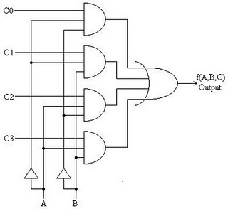
The working principle of the multiplexer circuit above is:
1. Value of bit 00 from the selector will choose the path of the first input as the output
2. Value of bit 01 of the selector will choose the path of the second input as output
3. Value of bit 10 of the selector selects the third input lines as output
4. Value of bit 11 of the selector will choose the four input channels as output
5. As long as there is no change in the bit selector logic condition of the output logic state also will not be amended.
6. If the line selector is connected with a series of counter-up the output to be obtained will represent the input lines in sequence.
7. So it can be concluded that the usefulness of the implementation of a multiplexer function is to satisfy the principle of a simple data distribution. Thus, with multiplexers is possible to transmit data remotely using only one connection.
Read More..
Where the above example can be seen that the circuit has 2 bit selector and 4 input lines. You can make a circuit with more input channels by increasing the number of bits of the selector. And also you can use a combination of gates based on your own design with reference to the previous multiplexer truth table you should specify. So by making a truth table in advance you can easily create a series of logic gates.
The working principle of the multiplexer circuit above is:
1. Value of bit 00 from the selector will choose the path of the first input as the output
2. Value of bit 01 of the selector will choose the path of the second input as output
3. Value of bit 10 of the selector selects the third input lines as output
4. Value of bit 11 of the selector will choose the four input channels as output
5. As long as there is no change in the bit selector logic condition of the output logic state also will not be amended.
6. If the line selector is connected with a series of counter-up the output to be obtained will represent the input lines in sequence.
7. So it can be concluded that the usefulness of the implementation of a multiplexer function is to satisfy the principle of a simple data distribution. Thus, with multiplexers is possible to transmit data remotely using only one connection.

Friday, November 7, 2014
LM723 Variable Power Supply with Over Current Protection
The circuit design was intended to create an adjustable power supply over a range of 1.3V to 12.2V at 1A and be able to provide protection for over-current by utilizing LM723 regulator.

Terminology
The integrated voltage regulator LM723 will supply 150 mA of output currents but any desired load current can be provided by adding external transistors for output currents in excess of 10A. This can be used as a linear or switching regulator since its output voltage can be adjusted from 2 Volts to 37 Volts while the input voltage can be at 40 Volts maximum. The range of variations of input voltage and load current can be kept at constant using this voltage regulator.
In this design, the DIL14 plastic packaged LM723 performs with 9.5V to 40V input DC voltage while having an output voltage that is not more then 6V to 7V below the input will lead to 150 mA current source from the IC. The difference between the input and the output DC voltage plus the current is proportional to the amount power being dissipated by the transistor T1 as it accepts all the current brought by the load, thus requiring a heatsink with a heat conductive value of 5K/W. T1 is made from 2N3055 which is intended for series and shunt regulators, for output stages and high fidelity amplifiers, and for power switching circuits. The output stage of the integrated circuit will be less loaded when an external pass transistor is used which will conduct at emitter-follower mode. This will in turn cause T1 to conduct at base-emitter mode thereby producing a major resistance in the IC.
Both ceramic capacitors must be positioned closer to the integrated circuit to prevent undesired oscillations, which the LM723 is prone to, since ceramic capacitors have high frequency coefficient of dissipation. Having these capacitors directly soldered would be too much for the IC since the operating temperature of the IC is in the range of -55ᵒC to +125ᵒC
Application
Voltage regulators are used for several advantages in areas where uncontrolled voltage varies more than the accepted voltage of equipment which could be harmful and damaging. In motor vehicles, it matches the charging requirements of the battery and electrical load to the output voltage of the generator by rapidly switching from one to another of three circuit states using a dual pole switch loaded with spring. To keep a recommended range of voltage supplied to a consumer, regulators are used by alternating current distribution feeders or large scale power distributions or substations. This is useful in protecting the equipment using electricity by minimizing the variations in voltage. The two types of regulators being used are step regulators where the current supply is controlled and the induction regulator where an induction motor adjust the voltage by supplying a secondary which smoothens the feeder line’s current variations.
The LM723 voltage regulators are widely used for wide range of applications such as a temperature controller, a current regulator, or a shunt regulator. Also, DC power supplies in electronic equipment are using voltage regulators.
Source:zen22142.zen.co.uk/Circuits/Power/723psu.htm
Read More..
Terminology
- LM723 – a positive NPN standard voltage regulator mainly designed for series regulator applications which can be utilized for both foldback and linear current limiting due to its very low standby current drain circuit
- Voltage Regulator – an electrical or electronic device created for the purpose of maintaining a constant voltage level of a power source within the suitable limits
- 2N3055 – a complementary Silicon Epitaxial-Base planar NPN transistor mounted in Jedec TO-3 metal case for use as power transistor
The integrated voltage regulator LM723 will supply 150 mA of output currents but any desired load current can be provided by adding external transistors for output currents in excess of 10A. This can be used as a linear or switching regulator since its output voltage can be adjusted from 2 Volts to 37 Volts while the input voltage can be at 40 Volts maximum. The range of variations of input voltage and load current can be kept at constant using this voltage regulator.
In this design, the DIL14 plastic packaged LM723 performs with 9.5V to 40V input DC voltage while having an output voltage that is not more then 6V to 7V below the input will lead to 150 mA current source from the IC. The difference between the input and the output DC voltage plus the current is proportional to the amount power being dissipated by the transistor T1 as it accepts all the current brought by the load, thus requiring a heatsink with a heat conductive value of 5K/W. T1 is made from 2N3055 which is intended for series and shunt regulators, for output stages and high fidelity amplifiers, and for power switching circuits. The output stage of the integrated circuit will be less loaded when an external pass transistor is used which will conduct at emitter-follower mode. This will in turn cause T1 to conduct at base-emitter mode thereby producing a major resistance in the IC.
Both ceramic capacitors must be positioned closer to the integrated circuit to prevent undesired oscillations, which the LM723 is prone to, since ceramic capacitors have high frequency coefficient of dissipation. Having these capacitors directly soldered would be too much for the IC since the operating temperature of the IC is in the range of -55ᵒC to +125ᵒC
Application
Voltage regulators are used for several advantages in areas where uncontrolled voltage varies more than the accepted voltage of equipment which could be harmful and damaging. In motor vehicles, it matches the charging requirements of the battery and electrical load to the output voltage of the generator by rapidly switching from one to another of three circuit states using a dual pole switch loaded with spring. To keep a recommended range of voltage supplied to a consumer, regulators are used by alternating current distribution feeders or large scale power distributions or substations. This is useful in protecting the equipment using electricity by minimizing the variations in voltage. The two types of regulators being used are step regulators where the current supply is controlled and the induction regulator where an induction motor adjust the voltage by supplying a secondary which smoothens the feeder line’s current variations.
The LM723 voltage regulators are widely used for wide range of applications such as a temperature controller, a current regulator, or a shunt regulator. Also, DC power supplies in electronic equipment are using voltage regulators.
Source:zen22142.zen.co.uk/Circuits/Power/723psu.htm
Monday, October 27, 2014
600 Watt Quasi Amplifier With Mosfet IRFP460
Two versions of a robust module capable of delivering high powwer for extended periods. The Actrk400 uses 6 n-channel Mosfets in the output stage to deliver around 400 watts into 4 ohms while the Actrk600 uses 12 n-channel Mosfets in the output stage to deliver power in excess of 600 watts into 4 ohms. One constructor has achieved almost 900 watts with the Actrk600 layout using 12 IRFP460 Mosfets.
 |
| 600 Watt Quasi Amplifier With Mosfet IRFP460 |
Tuesday, September 9, 2014
Subwoofer amplifier with 30W output power
Amplifier circuit is very suitable for use in subwoofer amplifier system based on IC SI1030G. Amplfier has 30W output with 8 ohm impedance. Supply voltage required minimum of 12 volts and a maximum of up to 22 volts DC.
Component List :
R1 = 100K
R2 = 1R
C1 = 2.2uF
C2 = 100uFC3 = 47uF
C4 = 100nF
C5 = 10uF
C6 = 47uF
C7 = 100uF
IC = SI1020GL , SI1030G
Power amplifier 450W with sanken
Circuit of power amplifiers with power output of 450 watts mono , amplifiers are also frequently used in the amplifier a high-power amplifier, which used in an event, in the field and the placed closed. Because this amplifier suitable for the woofer, fullrange speaker, and can also be fixed for the subwoofer speaker. To further strengthen and maximize the amplifier ,its power supply circuit also must be accurate, for electrolytic capacitors in power supply ,voltage capacitors use 80V or more, and a capcity 20000uF upwards, so when the bass amplifier is high , the voltage is not lot of experience dropping. Diode bridge use a minimum of 35A, or adjust the current input voltage. If the power supply has fulfilled the desire, the supply to the power amplifier.In the buffer circuit uses PNP transistor A1266 / A564 / A733 /A1015 / A798 and NPN with MJE340.To the driver circuit using PNP transistor MJE350 and MJE350. For the final amplifier circuit use two set 2SC2922 and 2SA1216. Use a quality sanken transistor to maximize quality sound output.Below is the amplifier and finshed PCB layout.


 |
| bottom view |
 |
| Top view |
If the track pcb does not look, you can download this series in the form of fort board, use the eagle cadsoft application to open it, but its components are not ordered , to their own satisfaction you can design it with your whishes.
Download file .brd here
 |
| Installation power amplifier |
 |
| This is power supply |
 |
| already amplifier |
Saturday, September 6, 2014
FM Moulator with IC 555
FM Modulator circuit is a simple FM modulation circuit using IC 555, where the resulting modulated signal has a tenuous meeting depends on the signal frequency information.
The resulting signal can be spelled out quite nice and stable so that the result will be more perfect. No winding or inductor in series modulator, so you do not need to bother to make a winding and calculate the value of the coil that you created it. With this circuit the desired value of frequency modulation can be obtained easily by calculating the frequency of IC 555 in general, which is determined by the resistor 6.8 K and 3.3 K and 0.1 UF capacitor. To obtain the other frequencies of your stay replace one or all three components.
Actually fm modulator ic 555 circuit is very simple though, but I think it reliable enough to handle a simple application purposes that do not require a big power or a very high frequency. But if you want more power you can add the RF amplifier circuit at the output of this circuit. Thus, the results of modulated signal can be amplified with the help of a series of supporters. In accordance with my experimental series modulators can work well at frequencies below the MHz range, because it is not IC IC 555 which is devoted to support of a very high frequency. You can use oscilltor transistor circuit, XTAL or others if you need a very high frequency.
The difference circuit with IC 555 on the multivibrator circuit in general is the use of pin 5, on the FM Modulator circuit is pin 5 of IC 555 is used as input information signal, which in turn will influence the shape of the output signal (modulated). But in applying this 5 pin multivibrator functions normally associated with 0.01 UF capacitor or left alone.
Thursday, September 4, 2014
5W power amplifier with IC TDA1016
This circuit use IC TDA1016 , minimum require voltage for this circuit 3 volt and maximum require voltage 15 volt .Its mono 5 Watt power output with impedance 4 Ohm , Current required 14 mA. In order for this circuit work optimally , the voltage should be at least 9 volts and the speakers should be higher 4 Ohm or equivalent, and use the speaker woofer. See Amplifier circuit schematic below :

Wednesday, September 3, 2014
Electronic Schmitt Trigger with Programmable Hysteresis Wiring diagram Schematic
Electronic Schmitt Trigger with Programmable Hysteresis Circuit Diagram. In electronics world, a Schmitt trigger is a comparator schema with hysteresis, implemented by applying positive feedback to the non inverting input of a comparator.
Electronic Schmitt Trigger with Programmable Hysteresis Circuit Diagram CA 3088 is used as a versatile Schmitt trigger. The size of the hysteresis levels is determined by Ia that flows out of the amplifier`s output and through R2. Increasing Ia increases hysteresis and vice versa. The positive and negative hysteresis levels are symmetrical about 0 V.
Electronic Schmitt Trigger with Programmable Hysteresis Circuit Diagram
USB SPDIF DAC with IC PCM 2902
The tool that I made and I discuss in this article I give the name USB SPDIF DACEvery word in the name corresponds to the function of the tool that I made this.
USB, this device serves to take the music information in digital form from a computer via the USB port
SPDIF, this tool can output digital music information received through the USB port, through the SPDIF output terminal that is also present in this device, so if you have a DAC that does not have a USB input, you can still use and do not need to buy a new DAC that has an input USB.
DAC, this tool can convert the digital signals derived from the USB port, an analog signal, which you can connect to the amplifier to the ahirnya you can hear the speaker
Scheme of the USB DAC can be seen in Figure 1 below.USB, this device serves to take the music information in digital form from a computer via the USB port
SPDIF, this tool can output digital music information received through the USB port, through the SPDIF output terminal that is also present in this device, so if you have a DAC that does not have a USB input, you can still use and do not need to buy a new DAC that has an input USB.
DAC, this tool can convert the digital signals derived from the USB port, an analog signal, which you can connect to the amplifier to the ahirnya you can hear the speaker
 |
| Click to view larger. | Figure 1 |
As you can see on the schematic in Figure 1 above, which is the heart of the circuit is IC USB DAC PCM2902 made by Texas Instrument, other than that I also added a digital SPDIF output isolation transformer on from this series. 2902 PCM encoding decoding work on the principle that generally abbreviated as word CODEC.
The new circuit will work when the USB input port terminal in the circuit connected to the computer, at this voltage 5V on the USB port of any computer will be triggering the circuit to begin work, and vice versa when the computer is turned off then the circuit will be in standby mode to wait until there is more tension 5V from USB port of computer.
When the received voltage is 5V USB port the computer then the circuit will begin to receive the digital data files during the grace period of 1 ms, all data received during the period of time of 1 ms is called a frame, the data in the first frame is stored in a memory buffer that is in the PCM2902, then the circuit will start the second frame as well as long lead times for 1mS, 1mS a second after the first data from the file will be converted into analog signals for analog terminal is then removed through out the pin 15 and 16 of the PCM2902, other than that this digital signal simultaneously will also excreted through the DOUT terminal pin 25 of the PCM2902 DAC to be connected to older products that do not have a USB input terminal.In addition to functioning as a DAC, PCM2902 actually also has other functions such as setting volume level and ADC, but the circuit that I developed is only aimed for the ADC and the conversion from USB to SPDIF.
Proposed Power Supply For USB SPDIF DAC
Power Supply that I use in this project using the configuration has been proven able to tame the hum in the tube 26, the power supply has karakater very stable, low noise and low impedance, but complicated to make, so for the purposes of this project I recommend another series that is not as complicated Heater power supply 26, but the quality is still better than most of the power supply kit used in the DAC in general, Figure 2 below is the recommendation power supply for USB DAC this project.
 |
| Click to view larger. | Figure 2 |
1. Diode bridge and capacitor input filter
2. TL431 as the reference voltage
3. OP Amp OP27 as the error amplifier
4. BD139 transistor as a pass transistorThis configuration is basically the general configuration of a linear regulator series, very much the regulator IC using this configuration, but the circuit in Figure 2 above has several advantages that are not owned by the regulator circuit in the form of ICa) high stability, since it uses a reference voltage source of good quality is TL431, and therefore not in a package with a pass transistor, the heat of the pass transistor can not seep into the source of reference voltage and makes it unstable, this sort of thing happens in IC voltage regulator.b) Using the Op Amp high quality, which in this case OP27, so it is not easy to oscillate as the OpAmp used in the regulator IC.c) If there is a chance you could also replace the TL431 or OP27 Op Amp voltage source and another that is expected to be better than either of these components.
 |
| Series of the finished PCB, top view |
 |
| IC PCM2902 |
Saturday, August 30, 2014
Simple USB player circuit with PCM2902
Usb series player is an electronic device or electronic circuit that functions as an MP3 player that is stored on a storage device such as USB flash.
In this usb circuit using an IC as a modifier of digital voice data into analog so that it can be applied to a headphone, or again through the power amlplifier strengthened so that it can be heard through the speakers. IC used in this circuit using IC PCM2902 as a modifier of a digital data into analog data storage.
Below is a schematic diagram of a USB player.
| Schematic usb player |
Thursday, August 28, 2014
FM Transmitter with two Transistor
Next date is the oscillator cum modulator date congenital about transistor Q2. Electrolytic capacitor C2 couples the achievement of the aboriginal date to the additional stage. R3 and R4 are the biasing resistors of Q2. R5 is the emitter resistor of Q2. Inductor L1 and trimmer capacitor C5 forms the catchbasin ambit which is all-important for creating oscillations. The articulate FM arresting is accessible at the beneficiary of Q2 and it is accompanying to the antenna application capacitor C9.
Notes.
- The circuit can be powered from anything between 6 to 12V DC.
- Using battery for powering the circuit will improve the performance and reduce noise.
- A 9V PP3 battery is a good option.
- If you are going with a battery eliminator, then it must be well filtered and regulated.
- Trimmer C5 can be used for adjusting the transmission frequency.
- Antenna can be a 1m copper wire.
- L1 can be constructed my making 4 turns of 1mm enameled copper wire on a 10mm diameter plastic former.
- Trimmer capacitor C6 can be adjusted for obtaining the maximum range.
- Most of the components required for this circuit can be procured from your junk box.
Wednesday, August 27, 2014
Multiplexer with CMOS IC 4556
In addition to the family of TTL ICs that support the function of a multiplexer is a family of CMOS ICs.
Read more
Read More..
Read more
Tuesday, August 26, 2014
0 4W power amplifier with 5G37 IC
This circuit requires a voltage of 6-12 Volts. To have a good quality of this series with the voltage necessary suplly good too. The definition of good that is filtered and does not release much ripple voltage and using large-capacity condenser elco issued for the bass is strong enough.
See below this circuit :
Datasheet IC 5G31A
Vcc = 6-12 V
Pout = 0,4 W
RL = 8 Ohm
Ft = 40-17 Khz
Icco = 15 mA
Package = TABS1-14
Manufactered = China
One LED with 9V Power

Hi every one you all know Free schema Diagrams 4U always give you easy and simple schema diagrams so today we are going to give you a special schema diagram.By using this schema diagram you can light up a LED with 9V

Sunday, August 24, 2014
Electronic Doorbell with Counter Wiring diagram Schematic
This schema is a doorbell with counter, that means it counts how many times the bell is triggered. It uses a chip synthesizer sound, the HT-2811 ms nothing prevents you from using another device sound generator. The HT-2811 reproduces the sound of a "ding-dong" doorbell. Besides this ic, the schema includes a CMOS 4026 and Display Driver IC which counts the total number of visitors.
Electronic Doorbell with Counter Circuit Diagram
Simple Electronic Data Circuit with LEDs
This is a given electronic schema with LEDs, to roll the dice just push the button. The electronics also ensures that no one can try to improve their lot by messing with the data. The key component of the data is a digital counter, an IC 4060 (IC1). This IC has a phase oscillator integrated so that only two resistors (R7, R8) and one capacitor (C7) is required to generate a clock.
Electronic Data Circuit with LEDs
The clock signal is divided, and the division is called CT in the design of IC symbol. For example, the output signal CT3 (pin 7) is a square wave with a frequency equal to the clock frequency divided by 23 (8). The clock signal is divided by 24 (16) in the outlet CT4 for 25 (32) CT5 output, and so on. This means that the output signals form a binary number.
Simple Voltage controlled current source with grounded source and load
This is a Simple Voltage controlled current source with grounded source and load. This is a simple, precise voltage-controlled current source. Bipolar supplies will permit bipolar output. Configurations featuring a grounded voltage- control source and a grounded load are usually more complex and depend upon several components for stability.Voltage-controlled-current-source-with-grounded-source-and-load. In this schema, accuracy and stability almost entirely depend upon the 100-0 shunt.
Voltage controlled current source schema diagram
Sourced by : Simple Voltage controlled current source with grounded source and load
Saturday, August 23, 2014
Fire alarm with light sensor
Fire alarm can be made with a light sensor (LDR) as in the article with the title of Fire Alarm with this LDR sensor. Principles of fire detection Fire Alarm with LDR sensor is to detect the presence of smoke through the LDR. LDR in the series Fire Alarm does not stand alone in detecting a fire, but the LDR in the pair with the light shining on the LDR.
Hence, in the detected smoke from the fire then the intensity of light received by the LDR LDR decreases and eventually trigger an alarm system on a series of Fire Alarm with this LDR sensor. Part 2 that in the series of Fire Alarm with Sensor LDR are some of the sensors, tone generator, audio power.
Image Series Fire Alarm with Sensor LDR

Function Section of the Fire Alarm with Sensor LDR
Part of LDR and light sensor facing to fire smoke detection
Part trigger using transistors and regulators as a trigger tone generator 7805
Tone generator section with IC UM66
Power audio section uses an audio power IC TDA 2002 which is equipped with voleme control (R3)
Friday, August 22, 2014
Power Supply 1 2 12V 1A with low voltage LED Indicator

This power supply can provide output voltage 1.2V - 12 with maximal output current is 1A, low voltage LED indicator added in this schematic diagram. The indicator part includes three diodes and one LED. For example you are charging a battery, you can observe the charge status at that moment. Another advantage of this schema, when the drawn current exceeds 1A (practically 0.85A), the current protector in LM317 intervenes and LED indicator warns you about the very low output voltage.
Thursday, August 21, 2014
1000W ICs audio amplifier with PA03
This is a series of amplifiers are based on the most high-ic power that I have ever known. Because the output is issued up to 1000 watts with the impedance RL 4Ohm. Current supply 120mA, and 30A output current. Minimum input voltage of about 30V and a maximum voltage up to 150V. This is an audio amplifier that I have come across use ICs that maximum voltage up to 150V and output power up to 1000W , the scheme below gan.
Part List
Resistor
R1 = 10K
R2 = 10K
R3 = 220K
R4 = 0.18R 5W
R5 = 2.2R 2W
R6 = 0.18R 5W
Capacitor
C1 = 1uF
C2 = 1000uF
C3 = 68pF
C4 = 1000uF
Inductor
L1 = 4MH
IC
U1 = PA03
Subscribe to:
Posts (Atom)
