Tuesday, August 12, 2014
Power Supply Balance Indicator Wiring diagram Schematic
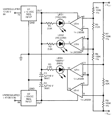
This schema uses two comparator pairs from an LM339N quad comparator; one pair drives the yellow positive (+)and negative (-)indicators, the other jointly drives the red warn LED3. The schema draws its power from the unregulated portion of the power supply. The four comparators get their switching inputs from two parallel resistor-divider strings. Both~strings have their ends tied between the power supply`s positive and negative output terminals.
The first string, consisting of R4, R5, and R6, divides the input voltage in half, with output taps at 0.5%. The other string, made up of R7, R8, and R9, also divides the input voltage in half, with taps at + lO%. The 0.5% R4/R5/R6 string drives the two comparators controlling the positive and negative indicators (LEDl and LED2). Their inputs are crossed so that LED2 does not fire until the positive supply is at least 0.5% higher than the negative; the positive indicator does not go off until the negative supply is at least 0.5% higher than the positive-in relative levels.
That overlap permits both LEDs to be on when the two supplies are in 1 % or better balance. The +lOT R7/R8/R9 string drives the other two comparators, which control the warn indicator. If either side of the supply is lO% or more higher than the other, one of the two comparators will switch its output low and light the redLED3the LM339N has opened-collector outputs, allowing such wired OR connections. The inputs are not crossed, as with the other comparator pair, so there is a band in the middle where neither comparators output is low and the LED remains off.
Power Supply Balance Indicator Circuit Diagram

Subscribe to:
Post Comments (Atom)
No comments:
Post a Comment