Sunday, August 31, 2014

Cheap Electronics Component for Amplifier Application

cheap
Cheap electronics component for amplifier application, it is simple to be made for speaker active . The sound quality even this  Mini Amplifier TDA2030 quite satisfactory for a portable audio system.


"The series of Mini Amplifier TDA 2030 "The series of mini amplifie can reproduce the power output of 14 Watt with 8 Ohm speaker load. The series of mini-amplifier can be supplied with ource voltage of 12 volts - 15 volts DC. more details, see the following series of pictures.

cheap

Daftar komponen
Resistor:

- R1: 150KΩ
- R2: 4.7KΩ
- R3: 100KΩ
- R4: 1Ω 1W
- RA/RB: 100KΩ

Capacitor

- C1: 1µF / 25V
- C2: 2.2µF / 25V
- C3: 100nF
- C4: 22µF / 25V
- C5: 100 µF / 25V
- C6: 220nF
- C7: 2200µF / 35V

IC / Dioda

- IC1: TDA2030 or TDA2030a
- D1/D2: IN4002
Read More..

Cash Box Guard

Most thefts happen after midnight when people enter the second phase of sleep called paradoxical sleep. Here is a smart security schema for your cash box that thwarts the theft attempt by activating an emergency beeper. The schema can also be used to trigger any external burglar alarm unit. The cash box guard schema (shown in Fig. 1) is built around IC CD4060 (IC1), which has an inbuilt oscillator and divider. The basic oscillator is configured by a simple resistor-capacitor (R-C) network. IC CD4060 divides this oscillator frequency into binary divisions, which are available as outputs.

In light, reset pin 12 of IC1 remains low, which enables the oscillator built around IC1. However, in the dark, it making all the outputs low. This also stops oscillations of the internal oscillator. Working of the schema is simple. If the cash box is closed, the interior will be dark. Hence in the dark, the light-dependant resistor (LDR1) resets IC1 and it stops oscillating and counting. At the same time, pins 13 and 14 of IC1 go low. So neither the piezobuzzer (PZ1) sounds, nor the relay (RL1) energises, indicating that the cash box is closed.

Cash Box Guard  Circuit Diagram
Cash
Fig. 1: Cash box guard schema

If someone tries to open the door of the cash box, light-most probably from the burglars pen torch -falls on LDR1 fitted into the cash box. As a result, LDR1 conducts and pin 12 of IC1 goes low. IC1 starts oscillating and counting. With the present timing R-C components (at pins 9, 10 and 11), the output timing at pin 14 of IC1 is two-three seconds. Hence pin 14 of IC1 goes high for two seconds after the door is opened and goes low for another two seconds. So the piezobuzzer (PZ1) sounds for two seconds and then falls silent for the following two seconds. This cycle repeats until the cash box is closed.

An optional relay is added for a remotely located audio/visual alert system. For that, a relay driver schema built around npn transistor BC548 (T2) is used. The relay is energised by the output from pin 13 of IC1 for about four seconds after the door is opened and then de-energised for the following four seconds. You can use this relay to activate another remotely located audio/visual alert system. After assembling the schema on a small PCB, house it in a small tamper-proof box (refer Fig. 2) leaving a little window for LDR1 and a small opening for the piezobuzzer (PZ1). Now fit the unit inside the cash box (refer Fig. 3) with LDR1 pointing towards the door of the cash box.


Fig. 2: Assemble unit

Note:
  1. The relay latching facility can be added to the schema by replacing transistor T2 with a suitable silicon-controlled rectifier such as BT169.
  2. By changing the value of resistor R1, you can adjust the light detection sensitivity of the schema.
  3. If you want to use a 3-pin piezobuzzer device, remove buzzer-driver npn transistor T1 and connect trigger pin of the buzzer directly to pin 14 of IC1. Also connect the positive and negative terminals of the buzzer to respective positive and negative points of the schema.
  4. Photo-transistor 2N5777 can be used in place of the 10mm LDR1.

Fig. 3: Unit fitted inside the cash box & also connected to an external alarm
Read More..

Installing a subwoofer in a pre fabricated enclosure

This guide will cover the installation of one or more subwoofers in a pre-fabricated enclosure. It will also cover the process of hooking up an amp to power the sub.

The easiest way to add low-end punch to your car’s stereo is to install a subwoofer. This guide will cover the installation of one or more subwoofers in a pre-fabricated enclosure. It will also cover the process of hooking up an amp to power the sub.


The first thing to do is to put the woofer into the box. This should be easy as long as you got the right size enclosure. Before actually screwing down the speaker, be sure to connect the included leads to the terminal in the back of the box. Next, screw the woofer down tight into the front of the box and mount the protective grille directly over the speaker.

Put the box in the trunk. For the best sound, the woofer should be facing the back of the car. To keep it from sliding around, consider using high-strength Velcro strips to secure it to the trunk floor. If this is not possible, L-brackets may be mounted to the cargo floor, but be sure not to put any screws through the side of the box. However you decide to secure it, make sure that it is out of the way of anything you put in the trunk.
Now it is time to install the amplifier. Begin by mounting the unit in the desired location. This should be a flat area with a lot of open space so that the amplifier can cool properly. Do not mount the amplifier on the subwoofer enclosure, as the vibrations from the speaker can damage the internal parts.

The next step is to hook the amp up to power. Before doing this, disconnect the negative terminal from the battery. Hook the long positive power cable for the amp to the positive terminal of the battery. If the cable does not have a fuse, you should install one inline within three feet of the battery connection. Consult the amplifier owner’s manual for the size of the fuse. Run the fused positive cable through the firewall and back into the cabin. Remove any trim panels necessary and pull back the carpet so you can run the cable underneath. Once the cable can reach the amp, trim off any excess, strip the end, and connect it to the positive power terminal of the amplifier. For the negative cable, connect it first to the amplifier, then run it beneath the cargo floor of the trunk and connect it to a ground point on the chassis or floor pan.
Next, you need to connect the amplifier to the head unit. You should do this using the subwoofer pre-amp hookup on your stereo. This can be either a stereo (paired RCA plugs) or mono (single RCA plug) connection. Unless you have a mono subwoofer amp, you will need to use a paired RCA cable to plug into the amp. If your head unit has a mono RCA out, this means you will need to use an RCA mono-to-stereo adapter to plug the stereo cable into the mono jack. Run the RCA cable underneath the carpet on the opposite side of the car from the power lines to avoid interference. When you get the cables back to the amplifier, plug them in at the RCA in terminals. Before putting the carpet and trim back, run a small 16-18 gauge wire from the head unit amp remote connection to the remote control terminal on the amplifier. At this point you can replace the carpet and trim panels to make the installation look clean.

The last step is to plug the subwoofer into the amplifier. To do this, use 12-14 gauge speaker wire. If you have a bridgeable stereo amp, you should bridge the amp by plugging the positive wire into the positive terminal for the left output and the negative wire into the negative terminal of the right output. The actual configuration of the bridge will vary from amp to amp, so read the owners manual for specific instructions. If you have a mono amp, simply connect the positive and negative wires. Finally, plug the wires into the back of the sub. If you have more than one sub, you can run a length of stereo from one sub terminal to the other.
Finally, put the negative terminal back on the battery and fire up your system. You will need to adjust the gain and filters on your amp, if it has them. First, turn on the low pass filter (LPF) option. Then, turn the gain all the way down. Turn up your stereo until the speakers begin to distort, then turn it down just a hair until it no longer distorts. With the stereo playing at this volume, turn up the gain on the amp just until the subwoofer begins to distort. At this point, turn the gain down a bit. That’s it; you’re done, and good luck with your new subwoofer.
Read More..

Simple Cell Phone Jammer Wiring diagram Schematic 2

A beautiful diy gsm jammer or mobile cell phone jammer schematic diagram for use only in GSM1900 with frequency from 1930 MHz to 1990 MHz. The GSM1900 mobile phone network is used by USA, Canada and most of the countries in South America.
 
This cell phone jammier is not applicable for use in Europe, Middle East, nor Asia. The GSM jammier schema could block mobile phone signals which works on GSM1900 band, also called DCS. For more cell phone jammers check the related posts.

Mobile cellphone jammer schema diagram


Read More..

Flat Battery Indicator Wiring diagram Schematic

This small schema was developed to monitor the battery in a model hovercraft. The lift in the model is produced by an electric motor driving a fan. To avoid the possibility of discharging the rechargeable battery pack too deeply, the design lights a conspicuous LED mounted on the model when a preset threshold voltage is reached. The schema only uses a few components, which helps keep the total weight of the model down. The schema connects to the model only across the two points where the voltage to be monitored can be measured. These also supply power to the schema.

The best place to connect the schema is not at the battery terminals, but rather at the motor connections. The schema is suitable for use with nominal battery voltages of 4.8 V to 9.6 V (four to eight 1.2 V cells). For example, if there are six cells in the battery, its nominal terminal voltage will be 7.2 V. A discharge threshold voltage of around 1 V per cell is appropriate, which means that for six cells the threshold is 6 V. We now need to set the voltage UZ across the adjustable Zener diode D1 (an LM431) to about 0.5 V less than the threshold voltage at which we want LED D2 to light.


Flat Battery Indicator Circuit Diagram


This voltage is controlled by the choice of the value of resistor R1. As indicated in the schema diagram, this is done with the help of a trimmer potentiometer (R1.A) with a fixed resistor (R1.B) in series. Using the suggested values (10 kΩ for both the potentiometer and the fixed resistor) allows the discharge threshold voltage to be set between about 5.5 V and 8 V. For lower or higher voltages R1.B should be made correspondingly smaller or larger. Once the desired value of UZ has been set the total resistance (R1.A plus R1.B) can be measured and a single fixed-value resistor of this value substituted at R1.

In the example mentioned of a six-cell battery, a voltage of 7.2 V will appear at the emitter of T1 when the battery is charged. At its base is UZ, which should be 5.5 V (6 V – 0.5 V) in the case of a discharge threshold voltage of 6 V. As long as the battery voltage remains at least 0.5 V higher than UZ, T1 will conduct and T2 will block, with the result that LED D2 will not light. If the battery voltage should fall below about 6 V (UZ + 0.5 V), T1 will block, T2 will conduct and LED D2 will light. To ensure stable operation of the schema R6 provides a small amount of switching hysteresis. By adjusting the resistor value between 100 kΩ and 220 kΩ the amount of hysteresis can be varied.

The current drawn by the schema itself is less than 5 mA (as measured with a battery voltage of 7.2 V). When the LED lights an additional 10 mA (the LED current) is drawn, for a total of around 15 mA. The adjustable Zener diode can be replaced by a fixed Zener with a voltage 0.5 V less than the desired threshold. Resistors R1 and R2 can then be dispensed with. A flashing LED can be used for D2 (without series resistor R7). An acoustic alarm can be provided by replacing D2 and R7 by a DC buzzer with a suitable operating voltage.

Source by : Streampowers
Read More..

Simple Electric Shock Gun Wiring diagram Schematic

This is a fantastic schema for self-protection. In case a burglar intrudes your house, you can use this security schema as a weapon for self-protection by giving a mild electric shock to the attacker.

This schema comprises astable multivibrator, inverter, and voltage quadrupler sections. The astable multvibrator is designed for 1 kHz with a 9V DC supply. The inverter section consists of switching transistors and an inverter transformer. The primary of transformer is of 9V-0-9V and the secondary is of 100V, 100mA. For compatibility, a driver transformer that is used in radio is used as the inverter transformer. The secondary output current of 100 mA gives a good enough shock to human body.

Simple
Fig. 1: Schematic diagram of toy shock gun

The astable multivibrator consists of two BC107 transistors (T1 and T2), two 0.01µF capacitors (C1 and C2), two 4.7-kilo-ohm resistors (R1 and R4), and two 72-kilo-ohm resistors (R2 and R3). A squarewave output of 1 kHz (with a phase shift of 180 degrees) is obtained at the collector of transistor T1 or T2. This squarewave output is given to the base of switching transistors BD139 (T3 and T4).

The collectors of transistors T3 and T4 are connected to the primary of the transformer and their emitters are grounded. A DC supply of +9V is also applied to the center-tapping of transformer X1 through switch S1. This is an inverter action, so we get around 100V AC at the secondary of the transformer. This AC is given to a quadrupler schema consisting of capacitors C3 through C6 and diodes D1 through D4.

Fig. 2: Barrel of the toy gun with the arrangement

The voltage quadrupler develops a DC voltage output equal to three or four times the input AC voltage. During the first positive half cycle, diode D1 conducts, charging C1 to Vm with polarity as shown in Fig. 1. During the first negative half cycle, diode D2 conducts, charging C2 to 2Vm. During the second positive half cycle, diodes D1 and D3 conduct, charging capacitors C1 and C3, while the voltage across capacitor C2 charges capacitor C3 to the same value 2Vm. During the second negative half cycle, diodes D2 and D4 conduct and capacitor C3 charges C4 to 2Vm. Thus, the voltage across C2 is 2Vm, across C1 and C3 is 3Vm, and across C2 and C4 is 4Vm. Therefore we get around 350V at the output of voltage quadrupler (across points A and B, as shown in Fig. 1).

Press the pushbutton switch (S1) of the schema and touch the output connectors to any object. There will be a heavy electric discharge, which is enough for a good shock.

The schema assembly and testing procedure is as follows:
1. Use a can type +9V battery for Vcc.
2. The transformer (X1) is designed to have 9V-0-9V primary and 100V, 100mA secondary, with primary winding having 80 turns (40+40, i.e. centre tapping at 40th turn) of 26 or 27 SWG and secondary winding having 450 turns of 35 or 36 SWG.
3. Mount the schema in a toy gun with output connectors at the front end of the barrel. The output connectors may be connected to two aluminium pieces with an insulator placed between them to avoid short schema. The arrangement is shown in Fig. 2.
4. Press switch S1 (here the trigger point of toy gun) and touch the front end of the barrel of toy gun to a person. The current in the voltage quadrupler will get discharged through the metal or aluminium pieces via the human body and the person will feel the electric shock.

The schema (excluding toy gun) costs around Rs 90.

Caution. Check the schema thoroughly before testing on anyone and use it judiciously, only when necessary.


Sourced By: EFY Author:  Praveen Kumar
Read More..

Basic LM35 temperature sensor circuit

 This is basic of workmaship LM35 temperatur sensor, whish is taken from the LM35 spending and boosted again by the amplifier op-amp. High output if the sensor is received by ic LM35 high temperature . You can use the output as driver relay, fan , or other. And if yo want to see modifications LM35 temperature sensor see here.


Read More..

Simple Power supply without transformer

Simple
This circuit has a voltage output of about 12 volts with 20mA current voltage. And this series of works using capacitive reactance and resistance are not using, this will reduce the heat on the circuit.


To be safe when there is a short-circuit series, always use a fuse on the input voltage is 220V. Here is a series of power supply without a simple transfomer.
Power
Power supply Circuit
Part List
R1 - 1.8K 1W
R2 - 100Ω
C1 - 0.47µF 400V
C2 - 1000µF 50V
D1 - 1N4007
D2 - 1N4007
D3 - 1N4007
D4 - 1N4007
ZD1 - 16V Zener Diode
ZD2 - 16V Zener Diode
ZD3 - 12V Zener Diode
Read More..

Saturday, August 30, 2014

USB Battery Charger Wiring diagram Schematic

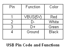
In recent years, the use of USB or Universal Serial Bus as a reliable communications interface in plenty of electronic devices have increased due to its increased speed, size and flexibility. It fundamentally consists of terminals VBUS(+5V supply), GROUND, D+ and D-. As plenty of of the devices run on rechargeable battery, it is now the trend to design the charging schema that makes use of the power supply from the USB port to charge the rechargeable battery. This feature will make the devices more convenient to the users as the devices will get their power from the bus and requires no outside plug or cables.


USB Bus Powered Functions
Theres fundamentally three classes of USB functions on power that can be derived from the port.

  High-Power Bus The high power bus powered functions derived all its power from the VBUS and cannt draw over 100mA until its been configured. One time configured, it can draw up to five unit loads(500mA) by requesting it in its descriptor. At full load, it must be able to work between the VBUS voltage of four.75V and five.25V.

  Low-Power Bus The low power bus powered functions derived all its power from the VBUS and must not draw over one unit load (100mA) according to the USB standard. It must even be able to work between the VBUS voltage of four.40V and five.25V.

  Self-Power Self power functions can draw up to 100mA from the VBUS and the rest from its outside source. This is the most simplest to design.

USB

USB Port Powered Battery Charger
This application schema makes use of the MCP73853/MCP73855 linear charge management controllers for cost sensitive applications. They are specially designed for USB applications and adhere to all the USB specifications governing the USB power bus. The schema below makes use of the MCP73855 to design a USB powered Lithium Ion/Lithium Polymer battery charger by deriving the power from the USB port.
Read More..

Vocal Eliminator Wiring diagram Schematic

Otherwise properly mixed sounds often suffer from a predominant solo voice (which might, of course, be the intention). Ifsuch a voice needs to be suppressed, the present schema will do the job admirably. The schema is based on the fact that solo voices are invariably situated `at the center` of the stereo recordings that are to be mixed. Thus, voice levels in the left- and right-hand channels are about equal. Arithmetically, therefore, left minus right equals zero; that is, a mono signal without voice. 

 Vocal Eliminator Circuit Diagram
Vocal

 There is, however, a problem: the sound levels of bass instruments, more particularly the double basses, are also just about the same in the two channels. On the one hand low-frequency sounds are virtu--ally nondirectional and on the other hand, the recording engineers purposely use these frequencies to give a balance between the two channels. However, the bass instruments can be recovered by adding those appearing in the left + right signal to the left-right signal. 

The whole procedure is easily followed in the schema diagram. The incoming stereo signal is buffered by A1 and A2. The buffered signal is then fed to differential amplifier A3 and subsequently to summing amplifier A5. The latter is followed by a low-pass filter formed by A6. You can choose between a first-order and a second-order filter by respectively omitting or fitting C2. Listen to what sounds best. The low-frequency signal and the difference signal are applied to summing amplifier A4. 

The balance between the two is set by PI and P2 to individual taste. You have noticed that the schema does not contain input or output capacitors. you wish, output capacitors can be added without detriment. However, adding input capacitors is not advisable, because the consequent phase shift would adversely affect the schema operation.
Read More..

Super High Power Portable TV and FM Jammer Wiring diagram Schematic

This is the Super High Power Portable TV and FM Jammer Circuit Diagram. There are still neighbors that keep annoying you by having loud the TV or the radio? Well I have you the solution. In fact all neighborhood will face your jamming waves at their TVs and radios, so be careful. 

This Jammer is the improved version of the old `TV and FM jammer schematic` with the difference of much higher power. Many of you where asking for a stronger and wider effect but to be as portable as can be. Looking at the schematic you can see that, only the parts are changing keeping the basic schema intact. Have in mind that this version needs heat sink and antenna to keep the transistor alive.

Super High Power Portable TV and FM Jammer Circuit Diagram

Super


The power source comes from three 9 volt batteries in series, so we use 27 volts at input, and we get a power full 2,5 Watts at output.  
 
You are going to need 70cm to 2 meter simple wire antenna.  
 
As for the transistor Q its the 2N3553. Its a RF Power Silicon NPN Transistor in a TO39 type  package designed to be used in amplifiers and oscillator applications in military and industrial equipment.
  
Usually found as an output driver, or in predriver  stages in VHF equipment, but because here we dont care about the modulation of the signal but just the power, thats why we use it as a first and final output driver. 
The transistor is specified at 175MHz and 28V to give: Output Power: 2.5W, Minimum Gain: 10dB and Efficiency: 50%. 
 
The parts are: R1=10k, R2=2,2K, R3=100 C1=47uF/50V, C2=2.2nF, C3=10pF, SW=switch, B=Battery 9V. 
 
The coil L should be closely wound 5 turns (start tunning with the closely wound distance of turns and then play with it and the C4 capacitor, to find the desired frequency )of enameled copper wire 1.5mm and internal coil diameter of 1cm (leads 2x20mm). 
 
The variable capacitor C4 should be air trimmer capacitor rating 4 to 30 pf or the closest to this value. 
 
Connect the batteries in series place the best heat sink for TO39 case you can get and pack it all in a small plastic box. Enjoy ;)


Datasheet file1: Click here to download 2n3553 datasheet.
Read More..

2004 Geo Tracker EV 2200 Wiring Diagram

2004 Geo Tracker EV 2200 Wiring Diagram
The part of 2004 Geo Tracker EV 2200 Wiring Diagram: batteries, deep cycle, controller, potentiometer, charger, fuel gauges, accessory battery, converter, voltage motor, voltage motor, ignition heater fault, fluid heater, ADC motor, gauge located instrument panel, front right engine compartment, panel illumination, relay box, clutch switch, fuel heater.
Read More..

NE5532 Headphone Amplifier

NE5532 Headphone Amplifier Circuit Diagram:

Partlist for NE5532:
P1 = 22K
R1 = 18K
R2 = 68K
R3 = 68K
R4 = 68K
R5 = 18K
R6 = 68K
C1 = 4.7uF/25v
C2 = 4.7uF/25v
C3 = 22pF
C4 = 220uF/25v
C5 = 220uF/25v
C6 = 4.7uF/25v
C7 = 22pF
C8 = 220uF/25v
J1 = 3.5mm Stereo Jack
B1 = 9V Battery
IC1 = NE5532
SW1 = SPST Toggle Switch
Read More..

18W MONO CLASS D AMPLIFIER

Features:

  • 18W OUTPUT POWER:
  • RL = 8Ω/4Ω; THD = 10%
  • HIGH EFFICIENCY
  • WIDE SUPPLY VOLTAGE RANGE (UP TO ±25V)
  • SPLIT SUPPLY
  • OVERVOLTAGE PROTECTION
  • ST-BY AND MUTE FEATURES
  • SHORT CIRCUIT PROTECTION
  • THERMAL OVERLOAD PROTECTION
Circuit Diagram:
Circuit diagram for 18W MONO CLASS-D AMPLIFIER

Read More..

Simple USB player circuit with PCM2902

Usb series player is an electronic device or electronic circuit that functions as an MP3 player that is stored on a storage device such as USB flash.

usb


In this usb circuit using an IC as a modifier of digital voice data into analog so that it can be applied to a headphone, or again through the power amlplifier strengthened so that it can be heard through the speakers. IC used in this circuit using IC PCM2902 as a modifier of a digital data into analog data storage.

Below is a schematic diagram of a USB player.
USB
Schematic usb player
Read More..

1997 Chevrolet Blazer Electrical Wiring Diagram

1997 Chevrolet Blazer Electrical Wiring Diagram
This is 1997 Chevrolet Blazer Electrical Wiring Diagram: Cruise Control System, Defogger, Rear Glass Release, Rear Wiper/Washer, Shift Interlock System, Transmission System, 6-Way Power Seat Circuit, A/C Circuit, etc. Computer Data Lines, Anti-lock Brake, Back-up Lamps Circuit, Charging Circuit, Keyless Entry, Engine Performance Circuits, Warning System, Courtesy Lamps, Door Lock Circuit, Electronic Transfer Case Circuit, Exterior Lamps, Front Wiper/Washer, Starting Schematics, Supplemental Restraint, Sealed Beam Headlamps, Horn, Instrument Cluster Circuit, Instrument Illumination, Power Distribution Circuit, Headlight, Ground Distribution, Power Mirror, Power Window, Power Window Diagram, Features: Power windows, power door locks, anti-lock braking, dual air bag, power mirrors, cruise control, air conditioner, AM-FM stereo radio with CD, 4.3-liter Vortec V-6 engine, four-speed automatic gearbox.
Read More..

Power Amplifier Protector

Now you can protect your HiFi amplifier from damage due to overheating. This circuit will cut off power to the amplifier board at the time the temperature was high. Automatically connect the power when the temperature returns to normal. This circuit uses a sensor NTC Thermister heat and also has a warning sound and reset determination.

Amplifier circuit protector is using popular timer IC NE 555 as the temperature controlled switch. The trigger pin 2 is connected to a potential divider consisting Thermister VR and NTC. Thus the voltage on pin 2 depending on the resilience and determination Thermister VR. NTC (Negative Temperature Coefficient) Thermister has a high resistance in the normal temperature and the resistance decreases as temperature increases. Threshold pin 6 of IC is used to reset the IC if necessary. When the pin 6 voltage gets higher than the IC pin 2 will reset and the output is low.

Power
Power Amplifier Protector  Circuits

Power to the amplifier board is given by (NC) contact is usually connected from the relay and the switch S2. So that power to the amplifier board will be available through the NC contacts of the relay when the relay S2 and the state is not powered. Thermister resistance is governed by VR triggering pin 2 of IC peaks at normal temperatures. When the temperature inside the cabinet amplifier increases, resistance decreases so that it becomes conductive Thermister. This makes the trigger pin 2 of IC is low and its output is high. T1 works so that the relay energizes and the ringing of a bell. This will damage the electrical supply to the amplifier board. Relay will not be automatically powered when the temperature returns to normal.

Amplifier circuit protectors are very useful to protect your home sound system.
Read More..

Friday, August 29, 2014

70 Watt OCL Amplifier Wiring diagram Schematic

OCL power amplifier schema used in the schema above is the type of power amplifier OCL (Output Capacitor Less) with a power output of 70 Watt. Circuit 70 Watt power amplifier OCL is working on a class AB with symmetrical voltage source of VCC ± 25 volts DC to ± 32 volts DC. OCL power amplifier schema uses a 70 watt power transistor complementary transistor TIP in 2955 and TIP 3055. 70 watt power amplifier in the schema can be used to drive the load (4-16 Ohm loudspeaker). Power supply schema power amplifier can use power supply schema with current 5A symmetrical. For stereo audio system needs to make a power amplifier OCL schema tone control + over 2 units.

70 Watt OCL Amplifier Circuit Diagram


70
Read More..

Simple Telephone Record Control

This schema will allow you to connect any tape recorder that has a mic and remote input to a phone line and automatically record both sides of a conversation when ever the phone is in use. You will need to take a couple of voltage readings before connecting the schema. First determine the polarity of your phone line and connect it to the schema as shown and then determine the polarity of the remote input and connect it to the schema. Circuit operation is as follows. When the phone is on hook the voltage across the phone line is about 48volts dc. When the phone is off hook the voltage will drop to below 10volts dc. When the line voltage is at 48volts the FET is off which causes Q2 and Q3 to be off. When the phone is picked up the FET turns on along with Q2 and Q3 which turns your recorder on. The tape recorder must be in the record mode at all times. As you can see the power source for the schema is the phone line.

Circuit Diagram

Read More..

Car subwoofer filter

Circuit description:
Here is the circuit diagram of a simple subwoofer filter that can be operated from a 12V DC supply. Such a circuit is very useful in automobile subwoofer applications. The circuit is nothing but a low pass filter whose pass frequency can be adjusted between 60 to 160 Hz. The circuit is designed around the TL072 dual BIFET opamp IC. Out of the two opamps inside the chip, IC1A is wired as a buffer. The left and right audio inputs after mixing is fed to the input of the IC1A using the DPDT switch S1. Switch S1 is the phase control switch which can be used to make the subwoofer in phase with other speakers. When S1 is in position 2, 180 degree phase shift will be induced.POT R7 can be used for controlling the level. IC1B forms the low pass filter whose pass frequency can be controlled by adjusting the dual gang POT R13.

Circuit Features:
  • The circuit can be powered from 12V DC.
  • IC1 must be mounted on a holder.
  • S1 is a DPDT switch.
  • R13 should be a dual gang linear POT.
  • C5 and C6 must be polyester capacitors.
  • POT R13 can be used for adjusting the pass frequency.
  • POT R7 can be used for adjusting the level.
Circuit diagram:

Car subwoofer filter

Read More..

DC Motor Speed Controller

DC Motor Speed Controller Circuit Diagram. This schema takes advantage of the voltage drop across bridge rectifier diodes to produce a 5-position variable voltage supply to a DC fan or other small DC motor. It is not as efficient as a switch-mode schema but it has the virtues of simplicity and no switching hash. The four full-wave bridges are connected so that each has two pairs of series diodes in parallel, giving a voltage drop of about 1.4V, depending on the load current.


dc-motor-speed-controller-schema
DC Motor Speed Controller Circuit Diagram

The rotary switch should have "make before break" contacts which should be rated to take currents up to about an amp or so. For higher currents, higher rated bridge rectifiers and a suitably rugged rotary switch (or solenoids) will be required. If you want smaller voltage steps, you could use the commoned AC inputs on the bridge rectifiers to give intermediate steps on the speed switch.

Author: Stephen Butcher,
Read More..

LED Christmas Star Wiring diagram Schematic

This schema can be used to construct an attractive Christmas Star. When we switch on this schema, the brightness of lamp L1 gradually increases. When it reaches the maximum brightness level, the brightness starts decreasing gradually. And when it reaches the minimum brightness level, it again increases automatically. This cycle repeats. The increase and decrease of brightness of bulb L1 depends on the charging and discharging of capacitor C3. When the output of IC1 is high, capacitor C3 starts discharging and consequently the brightness of lamp L1 decreases. IC2 is an opto-isolator whereas IC1 is configured as an astable multivibrator. The frequency of IC1 can be changed by varying the value of resistor R2 or the value of capacitor C1.

LED


Remember that when you vary the frequency of IC1, you should also vary the values of resistors R3 and R4 correspondingly for better performance. The minimum brightness level of lamp L1 can be changed by adjusting potentiometer VR1. If the brightness of the lamp L1 does not reach a reasonable brightness level, or if the lamp seems to remain in maximum brightness level (watch for a minute), increase the in-schema resistance of potmeter VR1. If in-schema resistance of potmeter VR1 is too high, the lamp may flicker in its minimum brightness region, or the lamp may remain in off state for a long time. In such cases, decrease the resistance of potmeter VR1 till the brightness of lamp L1 smoothly increases and decreases. When supply voltage varies, you have to adjust potmeter VR1 as stated above, for proper performance of the schema. A triac such as BT136 can be used in place of the SCR in this schema. Caution: While adjusting potmeter VR1, care should be taken to avoid electrical shock.
sourrce
Read More..

6 5W audio power amplifier

This amplifier circuit based on the ic, and the use here is that where ic STK4017 IC has output power of 6.5 watts with the impedance 8Ohm. Minimum required supply voltage and maximum 20Volt 35 Volt DC.
Read more
Read More..

LM4651 and LM4652 170W power amplifier

170 Watt power amplifier is a power amplifier that is built by IC LM4651 and LM4652.

Part of this power amplifier driver using the LM4651 IC designed specifically for the purpose of the class AB amplifier driver with short circuit protection feature, containing under voltage, thermal shutdown protection and standby functions. Section 170 Watt power amplifier using LM4651 IC with a MOSFET power amplifier is equipped with temperature sensors that will be used by IC LM4651 as controlnya thermal signal. IC IC LM4651 and LM4652 are designed specifically to each other in pairs to create a class AB power amplifier with protection features are detailed. Detailed series of 170 Watt power amplifier can be seen in thethe following figure .

LM4651

Power amplifier circuit requires supply voltages +22 V DC symmetrical 0-22V. Power Amplifier with IC LM4651 and LM4652 are often used in portable HiFi systems such as powered speakers, power subwoofer and car audio power Booter. D1, D2, D3 and D4 in series 170 watt power amplifier with LM4651 and LM4652 is a 22V zener diode.
Read More..

3 Input mic mixer circuit


This is a three input mixer.so you can use this to play your instruments or you can use this for small theaters.so try this.I have use this one for our special meetings.Total gain of the system is around 45decibel.


Note


# All inputs and output must be connected with respect to the ground.
# A +15/-15 V DC dual power supply is needed for powering the schema.
# Electrolytic capacitors C1, C2 and C3 must be rated 10V and other capacitors must be 30V.


Read More..

Oscillator Sine wave Wiring diagram Schematic

This schema is a sine wave oscillator which uses operational amplifiers working in oscillation back (positive feedback), or the oscillation output to the input. This oscillator is called Wien bridge schema is often used. The oscillator Sine wave oscillator is difficult to be done due to the distortion of the oscillation signal, different oscillator square wave, triangle wave oscillator (sawtooth).

Oscillator Sine wave Circuit Diagram

Oscillator


In the case of C1 = C2 = C, R = R1 = R2, giving the frequency of oscillation and can be calculated using the following formula.

Formula Sine Wave Oscillator


The example of the schema was made this time is shown below.
f = 1 / (2 x 3.14 x 10 -6 0.01 x 10 x 15 x 3)

f = 1 / (0.942 x 10 -3)
f = 1.062 x 10 3

f = 1062 Hz

The actual frequency of the schema was 900 Hz.
Read More..

Thursday, August 28, 2014

FM Transmitter with two Transistor

A lot of FM transmitter circuits accept been already appear here. This just addition one, a simple two transistor FM transmitter. The aboriginal date of the circuit is a preamplifier date based on transistor Q1. This is a beneficiary to abject biased amplifier date area resistor R2 sets the beneficiary accepted and R1 provided the all-important beneficiary to abject bias. C1 is the ascribe DC decoupling capacitor which couples the ascribe audio arresting to the Q1 base. C8 is the ability accumulation by-pass capacitor.

Next date is the oscillator cum modulator date congenital about transistor Q2. Electrolytic capacitor C2 couples the achievement of the aboriginal date to the additional stage. R3 and R4 are the biasing resistors of Q2. R5 is the emitter resistor of Q2. Inductor L1 and trimmer capacitor C5 forms the catchbasin ambit which is all-important for creating oscillations. The articulate FM arresting is accessible at the beneficiary of Q2 and it is accompanying to the antenna application capacitor C9.

Notes.
  • The circuit can be powered from anything between 6 to 12V DC.
  • Using battery for powering the circuit will improve the performance and reduce noise.
  • A 9V PP3 battery is a good option.
  • If you are going with a battery eliminator, then it must be well filtered and regulated.
  • Trimmer C5 can be used for adjusting the transmission frequency.
  • Antenna can be a 1m copper wire.
  • L1 can be constructed my making 4 turns of 1mm enameled copper wire on a 10mm diameter plastic former.
  • Trimmer capacitor C6 can be adjusted for obtaining the maximum range.
  • Most of the components required for this circuit can be procured from your junk box.
Read More..

Simple Noise Level Alarm Wiring diagram Schematic

Noise is a serious environmental problem that affects us in our daily life. There is scientific evidence supporting that noise exposure can cause hearing loss, hypertension, heart disease, annoyance, sleep disturbance and decreased performance in schools. Sound-level indicators like the one presented here can help address this problem. This sound-level indicator monitors the sound level and indicates through an LED when the level is above the preset value.


Circuit and working
Fig. 1 shows the schema of noise-level alarm. The schema is built around three BC550 npn general-purpose transistors (T1 through T3), electret microphone (MIC1), two LEDs (LED1 and LED2) and a few other components.

Simple Noise-Level Alarm Circuit Diagram


Simple
 Fig. 1: Circuit of noise-level alarm

The sound is captured by microphone MIC1 and amplified by first-stage high-gain transistor T1. Trimmer potentiometer VR1 is used to adjust the threshold level. the signal is amplified again with second-stage transistor T2. This amplified signal is rectified by diode D1 and the charge is stored in capacitor C10. Diode D1 should preferably be a small-signal Schottky diode such as BAT81, BAT82, BAT83, BAT85 or better. You can use 1N4148 and 1N914 also but the signal from the input should be stronger.

When the voltage across capacitor C10 is high enough, transistor T3 conducts and LED1 glows to indicate that the sound level is higher than the set level. LED2 indicates power supply is available to the schema.

Transistors T1, T2 and T3 should be high-gain type, such as BC550C, BC109C and BC108C. For powering the schema, you can use 6V from four AA-size batteries or 6V from a regulated wall adaptor.

Construction and testing
An actual-size, single-side PCB for the noise-level indicator is shown in Fig. 2 and its component layout in Fig. 3. After assembling the schema on a PCB, enclose it in a suitable case. Fix LED1, LED2 and potentiometer VR1 on the front panel.


Fig. 2: Actual-size, single-side PCB for noise-level indicator


Fig. 3: Component layout for the PCB


After connecting the 6V power supply to the schema, set the desired threshold of sound and adjust VR1 to the point where LED1 starts glowing. For that, switch on radio or TV set and set its volume to a level where you want the warning to start. Now adjust potentiometer VR1 to the point where LED1 starts glowing.

To test the schema for proper functioning, check correct input supply at TP1 with respect to TP0. LED2 also indicates the same. LED1 glows when the sound level is above threshold, which can be simulated with a radio or music system.

Sourced by : author  Petre Tzv. Petrov
Read More..

Inverter 12 V DC to 120 V AC

Inverter

This Inverter takes 12 volt d.c and steps it up to 120 volt a.c. The wattage depends on which transistors you use for Q1 and Q2, as well as the "Amp Rating" of the transformer you use for T1. This inverter can be constructed to supply anywhere from 1 to 1000 (1 KW) watts. If Q1, Q2 are 2N3055 NPN Transistors and T1 is a 15 A transformer, then the inverter will supply about 300 watts. Larger transformers and more powerful transistors can be substituted for T1, Q1 and Q2 for more power.


Parts
C1, C2 >> 68 uf, 25 V Tantalum Capacitor
R1, R2 >> 10 Ohm, 5 Watt Resistor
R3, R4 >> 180 Ohm, 1 Watt Resistor
D1, D2 >> HEP 154 Silicon Diode
Q1, Q2 >> 2N3055 NPN Transistor (see "Notes")
T1 >> 24V, Center Tapped Transformer
Misc:
Wire, Case, Receptacle (for output)
Fuses, Heatsinks, etc.

Note: Dont try to run inductive loads (motors...) off this inverter.
Read More..

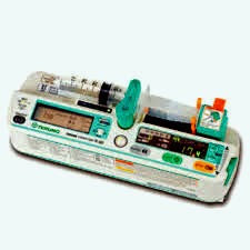
TERUMO TE331 TE332 Terufusion Syringe Pump E2PROM INITIALIZE and AGING

TERUMO TE-331 – TE332 Terufusion Syringe Pump. How to initialize E2PROM.
Medical (Electronic) Equipment.
E2PROM INITIALIZING
RAM data is erased and E2PROM is refreshed by ROM data [default data at factory].  This operation resets all the settings to the default.  Readjust required.
  1. Set the internal DIP switches 1 and 2 to ON and OFF respectively.
  2. While holding down the [STOP] switch, press the On/Off switch.  The display first shows “888.8”, then “FACt”, and a short beep follows.  Release the switches and check the display has changed to “”dIAg”; which stands for Diagnosis.  Note:  If you press the On/Off switch without pressing the Stop switch “Er91” appears on the 7 segment display.  Turn off the pump, and repeat the procedure above.  If you do not release the switches at the beep, the display changes to ‘Er 8”.  Once ‘Er 8’ appears, you have to turn off the pump, and repeat the procedure above.
  3. When “dIAg” is displayed, press the Display Select switch  3 times.  Check the display shows “CLEA” which stands for clear.
  4. Press ‘Stop ‘switch, and the display shows “E or J”.  E is for Europe, and J is for Japan.
  5. Press and hold PURGE’ switch about 1.5 seconds to choose ‘E for Europe’.
  6. Initialization of E2PROM starts.  The display changes to ‘Eur’.  As the initialization proceeds, first “      “, then “00     “,and “000 “, lastly “0000” appears on the display.the switch for Japan is the Start.  If the Start switch is pressed, “JP” appears on the display.
  7. When successfully completed, can hear a short beep and see the display of “good”.
  8. In case of failure, “bAd” is displayed.  Then the display returns to “CLEA”.
  9. Press On/Off switch to Exit the initializing E2PROM mode.
Aging.
  1. Set the DIP switches 1 and 2 to On and Off, respectively.
  2. While holding the Stop switch, press On/Off switch.  The display first shows “888.8”, then “FACt” and a short beep follows.  Release the switches and check the display has changed to “dLAg” which stands for Diagnosis.  Note: If you press the On/Off switch without pressing the ‘Stop’ switch “Er91” appears on the 7 segment display.  Turn off the pump, and repeat the procedure above.  If you do not release the switches at the beep, the display changes to “Er 8”.  Once “Er 8” appears, you have to turn Off the pump and repeat the procedure above.
  3. When “dIAG” is displayed, press the Display Select switch 4times.  Check the display shows “Aging”, which stands for Aging.
  4. Press Start switch, and Aging starts.
  5. When completed, press the On/Off switch to Exit the Aging Mode.
The following actions should be recognized while aging is performed.
* Motor rotates [slider moves approximately 9mm/h].
* All LED elements connected flash at 1 Hz / 50% duty.
* While the motor is rotating the minimum purge sound comes out.
AttentionYou can stop aging at any time by pressing the ‘Stop’ switch, and start again by pressing the Start switch.
* The motor stops if occlusion is detected with the load on the slider at approx. 4606N=4.7kgf.

Read More..

14 V battery charger circuit and troubleshooting

This circuit is also use operational amplifier IC LM324 to drive the VN64GA with the error signal and to control output voltage. This output voltage is pulsating DC , which is quite satisfactory for battery charging. This circuit also can be converted to the system regulated DC supply.
You do this by increased C2 and anoother electrolytic capacitor is added across the load. The respon time is very fast, determined by the op amp.
Schematic and troubleshooting below :
If the circuit not work , Perhaps the cause of :
  • AC cable disconnected
  • Transformer is damaged or leaking.
  •  Broken or leaky diode.
  • Installation of inverted foot elco.
  • Instrallation of the components of the upside , particularly on the transistor , examine the placement of the feet emitter , collector and base.
  • IC damaged.
  • Soldering is less sticky.
  • Line PCB damaged.
Read More..

Diode less Rectifier Wiring diagram Schematic

Diode less Rectifier Circuit Diagram . It`s common knowledge that when working with single-supply op amps, implementing simple functions in a bipolar signal environment can be difficult. Sometimes additional op amps and other electronic components are required. Taking that into consideration, can any advantage be attained from this mode The answer lies in this simple schema (A). Requiring no diodes, the schema is a high-precision full-wave rectifier with a liigli-frequency limitation equalling that of the op amps themselves. Look at the schema`s timing diagram (B) to see the principle of operation. The first amplifier rectifies negative input levels with an inverting gain of 2 and turns positive levels to zero .

The second amp, a noninverting summing amplifier, adds the inverted negative signal from the first amplifier to the original input signal. The net result is the traditional waveform produced by full-wave rectification. In spite of the limitation on the input signal amplitude (it must be less than VCCJZ), this schema can be useful in a variety of setups.

 Diode less Rectifier Circuit Diagram


Diode
Read More..

Fan Speed ​​Control for Temperature Wiring diagram Schematic

With this simple schema that you will be able to control the speed of a DC fan according to the temperature measured by a temperature sensor. It is an ideal accessory for your projects that require cooling that are not constant. 

This simple design allows precise speed control of motors, fans, and blowers, proportional to the temperature. An NTC thermistor (R1) is used as temperature sensor. A schema optional was added to remotely monitor the operation of the fan and to allow some kind of indication of the approximate speed by increasing the brightness of an LED.

 Fan Speed ​​Control for Temperature Circuit Diagram

 fan speed ​​control for temperature circuit diagram


The R5 must be configured to allow the engine just starting to run at the desired temperature. Any 6K8 between the NTC thermistor 22K can operate provided that the R2 value is one tenth of the thermistor. R6, R7 and D1 are optional: R7 obligation is adjusted until the LED glow dimly when the engine is just running.

Parts List
R1 15K @ 20 ° C NTC Thermistor (See Notes)
R2 1K5 1/4W Resistor (See Notes)
R3 1K 1/4W Resistor
R4 270R 1/4W Resistor 1/2W
R5 22K Trimpots
R6 680R 1/4W Resistor (Optional, see Notes)
R7 470R Trimpots
C1 100μF 25V Electrolytic Capacitor
LED D1 (Optional, any shape and color, see Notes)
Q1 BC547 45V 100mA NPN Transistor
Q2 BD140 80V 1.5A PNP Transistor
M1 Fan Motor 12V 700mA max.
Read More..

Pipe Bomb Mic Construction

Pipe Bomb Mic Construction, by Jamie Heilman:
My own dimensions for my prototype are X= 36cm, Y= 5.5cm. This imparted a fairly high pitch tone but I like it.


The X and Y dimensions really should be played with to develop the precise tone your seeking, also I chose a telephone loudspeaker as well as a crystal mic so I got the funkiest tone I could think of. A dynamic microphone might limit the treble somewhat most likely make it sound less harsh. I’d be considering any mods produced to this style (ie. stories, suggestions, etc.) so feel free to e mail me.

The amps may be any old easy op-amp construction that can drive a loudspeaker or take a mic input. I just made use of some excess material I had lying around to make mine. The end product had all the schemary inside the tube and the battery pack on the outside, with one control for the gain of the loudspeaker (mic was at fixed gain).

Note, in case you locate this in the front of the amplifier and turn every thing up, without having adding any dampening to the pipe, it will feedback just like you wont imagine! Youll most likely wish to keep away from this because it tends to hurt your ears. I put a bit of foam rubber in one end of the tube and an old sock in the other to dampen feedback. I like to leave my alternatives open though, so I also didn’t make this a permanent addition. My prototype is essentially a fuzz, as my guitar will overload the loudspeaker fairly simply and the pipe just adds a bit of strange overtone and what I believe is the smallest hint of reverb. Sounds excellent though! Clean tones via a similar set up would sound good too, but I haven’t constructed one of those yet. Possibly a larger speaker (4-5") and an old carpet pipe would probably add improved characteristics for clean tones. Attempt changing the tube material also for a various tone, I almost applied a bit of gutter piping when I 1st built this, right now I wonder what it would’ve sounded like.

Download the document about how to build Pipe Bomb Mic in PDF file:
Download Link
Read More..

Wednesday, August 27, 2014

Build a 1W Long Range FM Transmitter Wiring diagram Schematic

How to Build a 1W Long Range FM Transmitter Circuit Diagram. This is a simple1W Long Range FM Transmitter Circuit Diagram. This is a long range, very stable, harmonic free, FM transmitter schema which can be used for FM frequencies between 88 and 108 MHz. With good antenna transmitter can cover 5km range. 

 1W Long Range FM Transmitter Circuit Diagram


1W

It has a very stable oscillator because it uses LM7809 voltage regulator which is a 9V stabilized power supply for T1 transistor. Frequency adjustment is achieved by using the 10K linear potentiometer. The output power of this long range RF transmitter is around 1W but can be higher if you use transistors like KT920A, BLX65, BLY81, 2N3553, 2SC1970 or 2SC1971.
Read More..

MHz Oscillator using an ATtiny15 Wiring diagram Schematic

Most engineers will recognise the problem: Your schema needs a stable 1 or 2 MHz clock generator (in the author’s case it was for a Pong game using an old AY3-8500). A suitable crystal is not to hand so you cobble together an RC oscillator (there are plenty of diagram for such a design). Now it turns out that you don’t have exactly the right capacitor so a preset pot is add e d to allow some adjustment . Before you know it the clock schema is taking up more space on the board than you had hoped. 

Providing the application does not demand a precise clock source a tiny 8-pin microcontroller may offer a better solution to the problem. It needs no additional external components and an old ATtiny15 can be found quite cheaply. Another advantage of the solution is that clock frequency adjustment does not involve changing external components and is not subject to component tolerances. 

The microcontroller’s internal RC oscillator is already accurately calibrated to 1.6 MHz. With its inbuilt PLL, internal Timer 1 can achieve up to 25.6 MHz [2]. By configuring internal dividers the timer can output a frequency in range of roughly 50 kHz up to 12 MHz from an output pin. The difference between calculated and the actual output frequency increases at higher frequencies. A meaningful upper limit of about 2 MHz is a practical value and even at this frequency the deviation from the calculated value is about 15 %.

MHz Oscillator using an ATtiny15 Schematic

MHz
The schema diagram could hardly be simpler, aside from the power supply connections the output signal on pin 6 (PB1) is the only other connection necessary.The example program, written in Assembler is just 15 lines long! With a program this short comments are almost super fluous but are included for clarity. The code can be downloaded from the Elektor website [1]. 

The program only needs to initialise the timer which then runs independently of processor control to output the clock sign al . The processor can then be put into sleep mode to memory used up the remaining 99 % is free for use for other tasks if required. 

The OSCCAL register contains a calibration byte which allows some adjustment of the CPU clock. This gives a certain degree of fine tuning of the output frequency. A recommendation in the Atmel data sheet indicates that the CPU clock frequency should not be greater than 1.75 MHz otherwise timer operation cannot be guaranteed. 

The more recent ATtiny45 can be substituted for the ATtiny15. In this case the CK SEL fuses should be set to put the chip’s Timer 1 into ATtiny15- compatible mode [3]. After adjustment to the program it will now be possible to obtain a higher (or more exact) frequency from the timer, the ATtiny45’s PLL can operate up to 64 MHz.
Read More..

Booster BLW 60

In this post an opportunity, I upload booster BLW 60 which may be an inspiration to create home brew. Here I include a file layout that can be unlocked via software sprint layout. of course the software you can download here as well. ok g tuk need to talk at length, immediately wrote download the full data here


Read More..

Multiplexer with CMOS IC 4556

In addition to the family of TTL ICs that support the function of a multiplexer is a family of CMOS ICs.
Read more
Read More..

LTC3440 5V Boost Converter Circuit

A simple 5V boost converter using LTC3440 is shown here. LTC3440 is a highly efficient DC to DC converter which can be operated from input voltages below, higher than or equal to the output voltage. In terms of synchronous rectification, LTC3440 provides up to 96 efficiency and up to 600mA of output current is guaranteed. The IC contains a built in synchronizable oscillator whose frequency whose frequency can be adjusted from 300 KHz to 2 MHz.

In the circuit LTC3440 is wired as a 5V boost converter capable of delivering a steady 5V output @ 300mA from an input voltage from 2.7 to 4.2 V. Resistor R4 is employed to set the oscillator frequency while resistors R1 and R2 is employed to set the output to 5 volts. Resistor R3 and capacitor C1 forms a frequency compensation network while C3 serves as the input bypass capacitor. S1 is the shutdown switch and C2 is the output filter capacitor.
Read More..